


- News
14 January 2015
Reducing gate leakage and current collapse in GaN HEMTs on silicon
The University of Sheffield and the University of Cambridge in the UK have developed an optimized passivation for gallium nitride (GaN) high-electron-mobility transistors on silicon substrates (HEMTs) using sulfuric acid (H2SO4) treatment and silicon nitride (SiN) deposition [Z. H. Zaidi et al, J. Appl. Phys., vol116, p244501, 2014].
The researchers compared separate passivation efforts with sulfuric acid or hydrogen peroxide (H2O2) treatments, or 100nm silicon nitride deposition. They were particularly keen to tackle gate leakage currents and current collapse under pulsed operation with a view to power electronics applications.
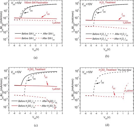
Figure 1: Gate transfer characteristics of AlGaN/GaN HEMTs before and after (a) 100nm SiN post-gate metal passivation, (b) H2O2 post-gate metal treatment, (c) H2SO4 post-gate metal treatment, and (d) H2SO4 pre-gate metal treatment.
The chemical treatments – hydrogen peroxide solution or sulfuric acid – reduced gate leakage current to less than 1μA/mm, improved the subthreshold swing (SS), and increased the on/off current ratio to around 107 (from 104-105), compared with silicon nitride deposition at 10V drain bias (see Figure 1). The researchers add: “Although the untreated devices showed a range of gate leakage currents, over the devices studied in this work, H2SO4 treatment was found to be the most effective in suppressing the gate leakage current and improving the SS.”
However, the peak drain current was reduced from 647mA/mm to 427mA/mm at 2V gate potential after sulfuric acid treatment. This treatment also shifted the threshold voltage furthest in a positive direction, although nowhere near enough to give enhancement-mode, normally-off operation.
The researchers comment: “These results suggest that H2SO4 treatment oxidizes the surface and, in the process, consumes some of the barrier layer (AlGaN), which in turn reduces the 2DEG charge. Formation of an oxide layer on the surface has a strong passivating effect and reduces the overall gate leakage current.”
In analyzing the sulfuric acid treatment’s effect on surface states, the researchers concluded that deep-level trap states are introduced that could have a catastrophic effect in normal switching operation, “causing a reduction in the total available drain current (current collapse) due to their sluggish response to changing bias”.
To overcome this problem, the team produced HEMTs with both sulfuric acid treatment and 100nm silicon nitride passivation (Figure 2). “This optimum configuration sustains a low gate leakage (<1μA/mm) with reduced sub-threshold slope (100+/-10mV/decade),” the researchers report.
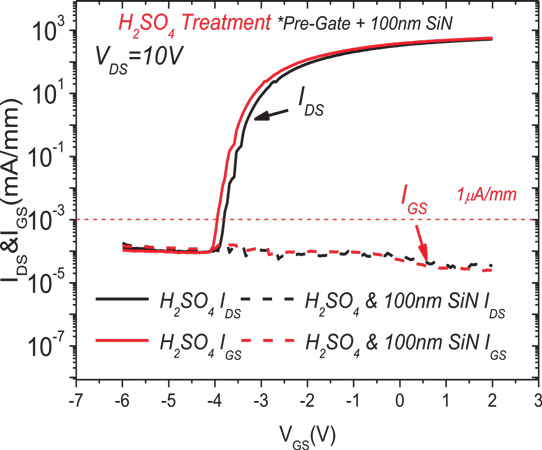
Figure 2: Gate transfer characteristics of AlGaN/GaN HEMTs with H2SO4 treatment combined with 100nm SiN passivation. Black curves are for pre-gate metal treatment and red curves are for treatment after gate metal deposition. In both cases SiN was deposited after gate metal.
Devices with just sulfuric acid treatment had a poor gate-lag ratio of 0.4+/-0.2 with 400ns pulses from a -6V gate off-state. The ratio increased to 0.85+/-0.1 in devices with combined sulfuric acid and silicon nitride passivation. This was almost identical with the performance of just silicon nitride passivation.
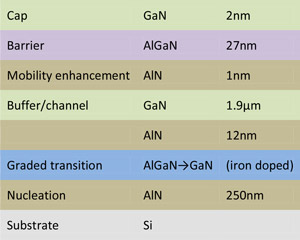 Figure 3: Epitaxial structure for HEMTs with aluminium gallium nitride barrier layer.
The epitaxial material (Figure 3) was grown on 6-inch (150mm) silicon wafers using metal-organic chemical vapor deposition (MOCVD). Standard HEMTs were fabricated with mesa isolation, titanium/aluminium/titanium/gold ohmic source-drain contacts, 1μm nickel/gold gates, and titanium/gold bond pads. The gate was centered in the 7μm gap between the source-drain contacts.
The 100nm silicon nitride passivation was achieved using plasma-enhanced chemical vapor deposition (PECVD). The hydrogen peroxide or sulfuric acid treatments were applied in solution at room temperature for around 48 hours. The sulfuric acid treatment was also tried before the gate formation, but then the researchers were naturally unable to compare performance before and after treatment.
GaN HEMTs on silicon GaN HEMTs SiN AlGaN MOCVD PECVD
http://dx.doi.org/10.1063/1.4904923
The author Mike Cooke is a freelance technology journalist who has worked in the semiconductor and advanced technology sectors since 1997.


