


- News
30 January 2015
Indium nitride surface quantum dots on silicon substrates
Researchers in Europe have studied indium nitride (InN) surface quantum dots (SQDs) produced on silicon substrates using plasma-assisted molecular beam epitaxy (PAMBE) [Paul E. D. Soto Rodriguez et al, Appl. Phys. Lett., vol106, p023105, 2015].
The team sees potential applications of the structures for future telecommunication and sensing devices. Also, indium gallium nitride on silicon (InGaN/Si) tandem solar cells and vertical contact schemes for nitride semiconductor devices could be achieved at much lower cost, it is hoped. Finally, direct integration with existing Si technology could be of much benefit in a number of nitride semiconductor technology deployments.
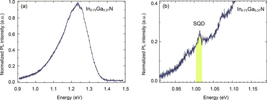
Figure 1: (a) Near-field PL spectrum from InGaN layer acquired at arbitrarily chosen position. (b) Selected near-field PL spectrum showing distinct emission peak from single SQD on low energy tail of InGaN emission.
The researchers were variously based at Universidad Politécnica de Madrid and Universidad de Cádiz in Spain, Max Planck Institute of Microstructure Physics and Universität Oldenburg in Germany, and Universitá di Milano-Bicocca in Italy.
The quantum dots were produced on (111) silicon. The nitrogen component was produced by a radio frequency active plasma source. The silicon substrate was prepared in the PAMBE reaction chamber by 4 hours of degassing (450°C) and 30 minutes of annealing (850°C).
Growth began with 5 minutes nitriding of the substrate surface with an active nitrogen flux at 850°C, followed by 1 hour with nitrogen (8.1x10¹³atoms/cm2-sec), gallium (4.4x10¹⁴atoms/cm2-sec) and indium (7.2x10¹⁴atoms/cm2-sec) fluxes at 450°C. The InN dots were produced by maintaining the nitrogen and indium fluxes for a further 10 seconds, giving about three monolayers of growth. The underlying compact In0.73Ga0.27N layer was 450nm thick.
Tapping-mode atomic-force microscopy (AFM) showed 100-200nm plateaus on which the InN dots formed uniformly. Dot diameters ranged between 10nm and 40nm with 2-4nm height. The density of dots was 7x10⁹/cm2. Closer high-resolution transmission electron microscopic (HR-TEM) analysis suggested that the dots formed on a 0.9nm InN wetting layer. The crystal structure of the wetting layer and the top portion of the dots was cubic. The underlying InGaN and bottom section of the dots were hexagonal. The cubic crystal structure could be beneficial in applications due to the absence of piezoelectric fields.
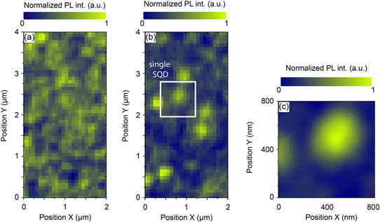
Figure 2: Near-field map of PL intensity acquired at 10K for (a) InGaN layer at energy 1.19eV outside energy region of SQDs, (b) individual SQDs integrated over energy range of 1.00-1.08eV, and (c) single SQD with enlarged magnification integrated from 1.005eV to 1.020eV.
At arbitrary locations, near-field overview photoluminescence showed a broad peak around 1.23eV. At selected positions, narrow peaks in the range 0.95eV-1.10eV were also seen, which the researchers "tentatively" attribute to emission from distinct dots. The narrow peak width was around 15meV. However, the density of emitting dots was lower than the AFM density, suggesting that not all the dots were optically active.
The InN dot line widths were wider than the μV levels seen with the highest-purity InGaN dots. Charged surface states are seen as a potential cause of the line broadening of the InN dots on silicon. The researchers comment: "Temporal variations in the charge distribution within these states give rise to fluctuating electric fields in the confined SQDs and thus to a line broadening in continuous wave PL measurements. InN has the highest density of charged surface states among all semiconductors and such line broadening effects are, therefore, particularly pronounced."
The team suggests that the sensitivity of the InN dot energy states to these surface charge states could lead to high-performance sensors.
Indium nitride surface quantum dots InN Silicon substrates PAMBE
http://dx.doi.org/10.1063/1.4905662
The author Mike Cooke is a freelance technology journalist who has worked in the semiconductor and advanced technology sectors since 1997.


