


- News
8 July 2015
High-temperature recess for normally-off gallium nitride transistors
Researchers in China and Hong Kong have claimed the highest output power density and power-added efficiency reported to date for gallium nitride (GaN)-based enhancement-mode metal-insulator-semiconductor high-electron-mobility transistors (MIS-HEMTs) at 4GHz and in pulsed-mode [Sen Huang et al, IEEE Electron Device Letters, published online 15 June 2015].
Enhancement-mode or 'normally-off' devices are desired for radio frequency (RF), microwave and power applications, giving fail-safe operation and simpler gate control. Unfortunately, without special processing, GaN HEMTs tend to be 'normally-on'/depletion-mode.
Gate recessing and the addition of a gate dielectric can produce enhancement-mode devices with high transconductance and low gate leakage. Gate recessing requires some form of etch, which can introduce lattice damage. Also, the etch process can leave residues. Both these factors can introduce electron trap states that negatively impact performance.
The team from Chinese Academy of Sciences' Institute of Microelectronics, Xidian University, and Hong Kong University of Science and Technology (HKUST) have developed a high-temperature plasma etch that removes residues and recovers lattice damage.
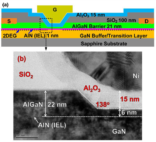
Figure 1: (a) Schematic device structure of E-mode Al2O3/AlGaN/GaN MISHEMTs. (b) TEM cross-sectional view of gate edge of E-mode MISHEMTs with gate recessed at 180°C.
The epitaxial material for the device (Figure 1) was grown by metal-organic chemical vapor deposition (MOCVD) on sapphire. The 21nm Al0.25Ga0.75N barrier was grown on a 1nm AlN interface enhancement layer on GaN buffer. The sheet resistance of the AlGaN/GaN heterostructure was 310Ω/square (1980cm2/V-s mobility).
The ohmic source-drain contacts were fabricated with titanium/aluminium/nickel/gold metalization, annealed at 870°C in nitrogen for 50 seconds. Passivation and etch masking was provided by 100nm silicon dioxide from plasma-enhanced chemical vapor deposition (PECVD).
Gate recessing was performed after mesa isolation. The low-RF-power mixed chlorine/boron trichloride inductively coupled plasma (ICP) etch for the gate recessing was performed at 180°C. "The high temperature enables effective desorption of chlorine-based etching residues, e.g. AlCl3, GaCl3, and NCl3," the researchers explain. The recess depth was about 16nm into the AlGaN barrier.
The recessed gate region was covered with 15nm aluminium oxide gate dielectric from a thermal-mode 300°C atomic layer deposition (ALD). The precursors were trimethylaluminium and water/ozone. The water precursor was used for the first 2nm and the ozone for the remaining 13nm. The use of the water precursor avoided oxidation of the AlGaN barrier. A post-deposition anneal was carried out at 500°C for 1 minute in nitrogen.
The gate electrode was nickel/gold with 1μm length, 100μm width, and 1μm overhangs toward the source and drain electrodes. The gate-drain and gate-source separations were 3μm and 2μm, respectively.
Devices produced with the high-temperature (HT) recess process have similar threshold voltages compared with MISHEMTs from room-temperature (RT) recessing. However, the HT-MISHEMTs have smaller hysteresis in double-mode characteristics, suggesting "significant suppression of deep interface/bulk traps". The OFF-state standby power for the HT-MISHEMT was 6x10⁻⁸W/mm for 0V gate and 30V drain.
In small-signal RF measurements on the HT-MISHEMT at 10V drain bias and 2.5V gate, the current-gain cut-off (fT) was 7.6GHz and the unit power gain (fmax) came at 27GHz. The maximum values for the RT device were 5.4GHz and 14.9GHz.
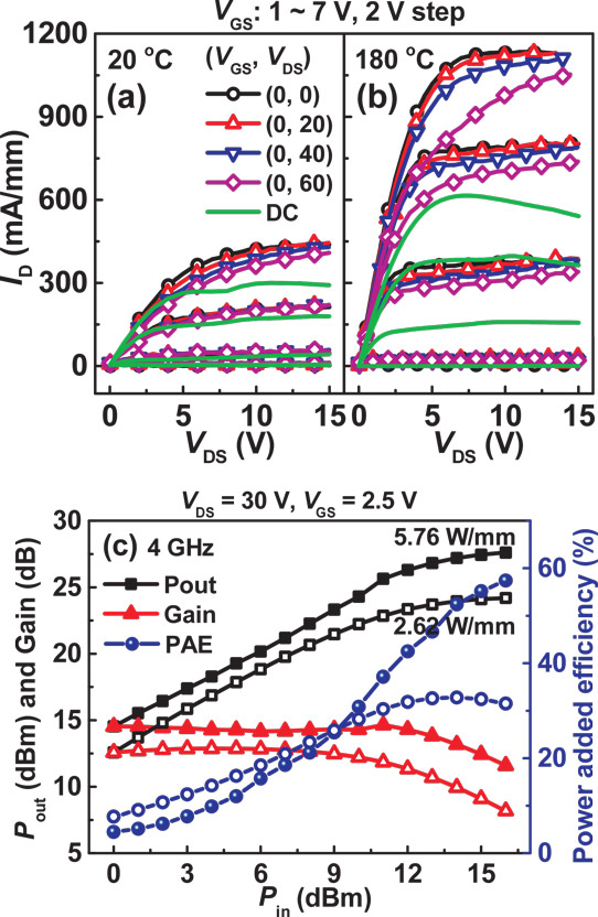
Figure 2: Pulsed ID-VDS characteristics of E-mode Al2O3/AlGaN/GaN MISHEMTs with gate recessed at 20°C (a) and 180°C (b). (c) ON-wafer large-signal RF characteristics (4GHz) of E-mode MIS-HEMTs with gate recessed at 180°C (solid symbols: pulse-mode; open symbols: continuous-wave).
Pulsed operation at 7V gate gave 1.13A/mm drive current for the HT device, while the RT-MISHEMT could only manage 0.42A/mm (Figure 2). The researchers comment: "The pulsed currents are much higher than the corresponding dc output current in both devices. There may be some trapping mechanisms other than self-heating effect that is responsible for the degradation of IDmax, and these trapping processes only appear in quasi-static dc measurement."
The current collapse effects are small at quiescent drain biases below 40V, but are large at 60V. The researchers comment: "It is probably caused by oxidation-induced deep interface states (at the PECVD-SiO2/AlGaN and/or ALD-Al2O3/AlGaN interfaces)." They also believe that the interface properties could be improved with crystalline AlN passivation.
Large-signal 4GHz RF power performance was measured with class AB biasing. Output power was 5.76W/mm at the 3dB compression point in pulsed mode. In continuous-wave operation, the output was 2.62W/mm, compared with 1.05W/mm for the RT-MISHEMT. The power-added efficiencies for the HT-MISHEMT were 33% for continuous wave and 57% in pulsed mode.
http://dx.doi.org/10.1109/LED.2015.2445353
The author Mike Cooke is a freelance technology journalist who has worked in the semiconductor and advanced technology sectors since 1997.


