


- News
22 July 2015
Cutting leakage in gallium nitride vertical diodes on silicon
Researchers in the USA have developed vertical Schottky and pn gallium nitride (GaN) diodes on silicon with performance comparable to devices grown on much more expensive substrates [Yuhao Zhang et al, IEEE Transactions On Electron Devices, vol.62, p2155, 2015].
The researchers from Massachusetts Institute of Technology (MIT), and from Synopsys Inc and Applied Materials–Varian, worked in particular to reduce reverse leakage currents from a number of sources.
Lateral GaN diodes have been widely developed but suffer from reliability and integration challenges. Vertical devices could be able to handle higher voltages with a smaller footprint. Also, vertical devices should benefit from a structure where the peak field is away from the surface of the diode, along with better thermal performance.
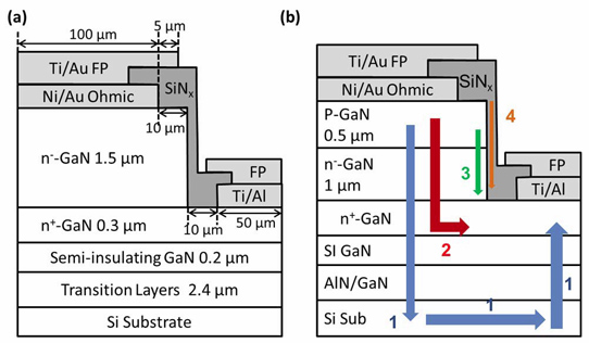
Figure 1: Schematic of GaN-on-Si vertical (a) Schottky and (b) p-n diodes. Four possible leakage paths in GaN-on-Si vertical diodes are shown in (b).
The heterostructures for the Schottky and pn diodes (Figure 1) were grown on (111) silicon using metal-organic chemical vapor deposition (MOCVD). The devices were fabricated by etching 1.6μm cathode electrodes from the top GaN layers, and depositing cathode and anode ohmic contacts, 200nm silicon nitride passivation and field plates. Titanium/aluminium were used for the cathode contact ring and field plates. The circular anode contact consisted of nickel/gold.
The researchers investigated four possible routes of current leakage: "1) through the transition layers and Si substrate; 2) through the drift layer; 3) along the etch sidewall; and 4) through the passivation layer."
Tests with trench structures suggested that leakage path 1 was negligible. Also, improvements in the silicon nitride passivation at MIT have reduced path 4 currents to a similarly negligible level. The improvement involves using sputtering rather than plasma-enhanced chemical vapor deposition (PECVD) [www.semiconductor-today.com/news_items/2014/MAY/MIT_060514.shtml].
Inductively coupled plasma etch damage (giving defects such as nitrogen vacancies) tends to lead to leakage through path 3. Such etches can change a p-GaN surface into a depleted or n--GaN region, giving reverse bias leakage.
To overcome the etching problem, an edge termination process was developed to repair dry etch damage that combined carbon tetrafluoride or nitrogen plasma treatment, tetramethylammonium hydroxide (TMAH) wet etching, and argon ion implantation. The ion implantation ring isolated the main vertical current from the etch sidewall (Figure 2).
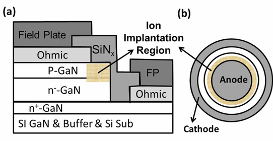
Figure 2: (a) Cross section and (b) top view of the GaN-on-Si vertical p-n diodes with ion implantation regions as edge termination.
By creating diodes of various diameters, the researchers concluded that the edge termination process effectively suppressed leakage through path 3, leaving bulk leakage through path 2 as the main contributor.
The reverse leakage in the enhanced pn diodes was reduced by two orders of magnitude, while maintaining a soft breakdown voltage of more than 300V (peak field estimated at more than 2.9MV/cm). The 300V soft breakdown performance is close to the theoretical maximum for a 1.5μm thick drift layer. Thicker GaN layers should increase the breakdown voltage.
Schottky and pn diodes of 600μm-diameter demonstrated forward currents of more than 2A (500A/cm2) in pulsed measurements with duty cycles up to 1%. The on-resistance for 600μm-diameter Schottky diodes was 6mΩ-cm2 – for similar pn diodes the resistance was higher at 10mΩ-cm2.
The researchers comment: "The relatively high ON-resistance of our GaN-on-Si vertical diodes is due to the relatively high contact resistance of ohmic on p-GaN, low mobility of p-GaN (14cm2/V-s), and the current crowding near the corner of etching sidewall. An improvement of the p-GaN material quality is expected to further reduce the ON-resistance of our GaN-on-Si vertical diodes."
Table 1: Leakage and cost benchmarking for the GaN vertical device on different substrates, GaN lateral device, Si and SiC device.
| Diode | Leakage current (density) at -200V | Ion/Ioff ratio | Available substrate | Substrate cost per cm2 |
| GaN-on-Si vertical (this work) | < 1μA (10-4-10-3A/cm2) | ~106 | 200mm Si | ~$0.08 |
| GaN-on-sapphire vertical | 10-3A/cm2 | ~105 | 100mm sapphire | ~$2.2 |
| GaN-on-GaN vertical | 10-5—10-6A/cm2 | ~109 | 50mm GaN | ~$100 |
| AlGaN/GaN lateral | 10-2A/cm2 | ~105 | 200mm Si | ~$0.08 |
| Si (NTE 588) | 5μA | ~106 | 200mm Si | ~$0.08 |
| SiC (APT6SC60K) | < 1μA | ~106 | 75mm SiC | ~$6 |
| Si power MOSFET (IRHNJ597230) | > 10μA (10μA at -160 V) | ~106 | 200mm Si | ~$0.08 |
The researchers compared their device performance with diodes produced on more expensive substrates (Table 1). They comment: "With over 1000× lower substrate cost than the GaN-on-GaN device, our GaN-on-Si vertical devices achieved an OFF-state leakage current lower than the GaN lateral devices and similar to the one in the state-of-the-art Si and SiC devices."
http://dx.doi.org/10.1109/TED.2015.2426711
The author Mike Cooke is a freelance technology journalist who has worked in the semiconductor and advanced technology sectors since 1997.


