


- News
10 July 2015
Vertical Schottky barrier diodes on free-standing gallium nitride
Japan's Toyoda Gosei Co Ltd has developed vertical gallium nitride (GaN) Schottky barrier diodes (SBDs) capable of handling 50A forward current with 790V reverse blocking [Nariaka Tanaka et al, Appl. Phys. Express, vol8, p071001, 2014]. "To our knowledge, the characteristics of operation with a simultaneous high forward current and high blocking voltage are reported for the first time for vertical GaN SBDs on free-standing GaN substrates," the researchers comment.
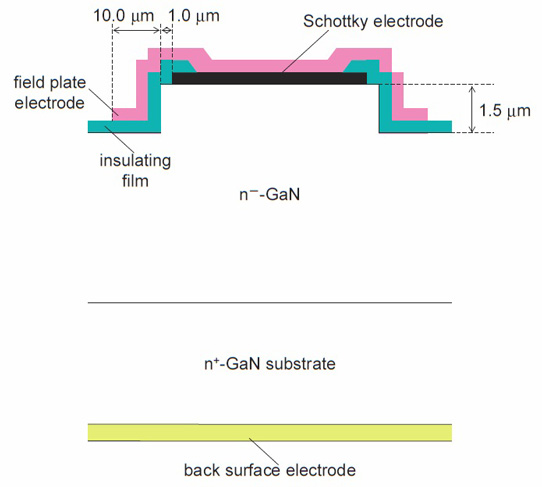
Figure 1: Vertical GaN SBD.
Metal-organic chemical vapor deposition (MOCVD) was used to create a 10μm lightly doped n--GaN layer on commercially available free-standing heavily doped n+-GaN substrate. The SBD (Figure 1) consisted of mesa isolation, nickel Schottky anode, insulating film, aluminium-based field-plate, and aluminium/titanium back-contact cathode. The insulating film was 500nm silicon dioxide and 100nm aluminium oxide. The field-plate was designed to relieve potential crowding at the edge of the Schottky electrode. Potential crowding increases leakage current and reduces blocking voltages.
A 3mmx3mm device managed a 50A forward current with a bias of 2.05-2.25V. The researchers expect that higher currents can be achieved since their equipment was limited to 50A. The differential on-resistance above 20A was 25-29mΩ. Since this value was very close to estimates based on the resistivity of the GaN material, the researchers believe the contact resistance with the back-electrode was negligible.
The blocking voltage under reverse bias was 730-790V. Repeat measurements showed the breakdown to be non-catastrophic. The researchers believe that the combination of high forward current and high reverse blocking is a first for vertical SBDs on free-standing GaN.
The reverse blocking was about 200V short of a simple prediction based on thermionic field emission theory. The researchers comment that the difference could be due to potential crowding at the Schottky electrode edge, dislocations, or a combination of the two.
Experiments with different area Schottky diodes showed the forward current density behavior with respect to voltage up to 0.5V to be very similar down to 200μm dimensions. The Schottky barrier height was estimated at 1.01-1.02eV and the ideality was 1.01, according to the thermionic emission model.
The reverse current density versus voltage was also similar across the different area SBDs. Since the higher-than-expected reverse leakage was thought to be due to either potential crowding or dislocations in the bulk material, the researchers tried to disentangle the effect by seeking the behavior of the leakage according to the perimeter (edge) or area (bulk) of the device. In particular, the leakage at 400V reverse bias was plotted against the perimeter-to-area ratio (Figure 2). Since the effect of the perimeter was small, the researchers concluded that perimeter current was small compared with the bulk current.
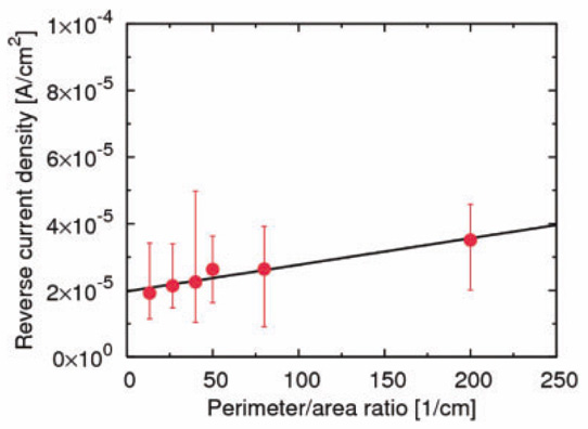
Figure 2: Reverse current density at 400V as a function of perimeter/area ratio.
The researchers believe that improving the n--GaN growth process will enable the achievement of higher reverse blocking voltage combined with the same high forward current.
Vertical Schottky barrier diodes Free standing GaN GaN MOCVD
http://dx.doi.org/10.7567/APEX.8.071001
The author Mike Cooke is a freelance technology journalist who has worked in the semiconductor and advanced technology sectors since 1997.


