


- News
1 July 2015
Grading gallium indium nitride arsenide for multi-junction solar cells
Researchers based in Germany and the UK have been developing growth processes of gallium indium nitride arsenide (GaInNAs) with graded composition for use in multi-junction solar cells [F. Langer et al, Appl. Phys. Lett., vol106, p233902, 2015]. The grading produced a slanted bandgap of 39meV across a 1μm absorber layer that enhanced the extraction of photo-generated carriers from 34.0% to 36.7% in the 900-1100nm wavelength range.
Lattice-matched GaInNAs 1eV bandgap layers could extend the performance of standard monolithic multi-junction devices of gallium indium phosphide/gallium indium arsenide/germanium. However, the introduction of nitrogen into the GaInAs structure tends to introduce deep-level defects that increase residual carrier densities from ~1015/cm3 to the mid-1016/cm3 range, inhibiting the extraction of photo-generated carriers. By grading the GaInNAs composition, photo-generated carriers can be extracted more efficiently.
University of Würzburg and University of St Andrews grew their heterostructures by molecular beam epitaxy (MBE) with the nitrogen supplied as radio-frequency plasma and the other atomic species generated by solid sources. The substrates were zinc-doped (100) GaAs wafers offcut 6° to the (111)B plane.
Layers of Ga1-xInxNyAs1-y were grown at 380°C. Different compositions were achieved through control of the flux from the Ga solid-source effusion cell. Lattice matching with the underlying GaAs was achieved by keeping the x fraction at about 3x the y fraction. A post-deposition anneal was carried out at 700°C.
Table 1: Grown Ga1-xInxNyAs1-y films.
| Sample | x/Δx | y/Δy | Eg/ΔEg | Lattice mismatch |
| A | 0.069/0 | 0.0230/0 | 1.050eV/0 | 0.012% |
| B | 0.075/0 | 0.0250/0 | 1.038eV/0 | 0.005% |
| C | 0.083/0 | 0.0277/0 | 1.011eV/0 | 0.008% |
| A→C | -/0.014 | -/0.0047 | -/0.039eV | 0.027% |
| A→B | -/0.006 | -/0.0020 | -/0.012eV | 0.005% |
Various ungraded and graded 1μm layers of GaInNAs were grown on 200nm GaAs buffer (Table 1). The structure was completed with a 100nm GaAs cap.
The researchers believe that the main effect of the grading is felt by the conduction band rather than the valence band. Hence, the grading will mainly affect the behavior of photo-generated electrons. Photoluminescence through the cap and substrate supported this picture (Figure 1).
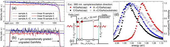
Figure 1: (a) and (b) Depth profiling by secondary-ion mass spectrometry and linear fits of N and In content in GaInNAs layers. (c) Schematic energy band lineup of sample A→C. (d) Photoluminescence spectra obtained under 980nm excitation.
Compositional grading processes were used to create solar cells with p-i-n diode structures (Figure 2). Aluminium gallium arsenide (Al0.25Ga0.75As) was used for 50nm blocking layers. The active GaInNAs material was 1250nm – 1000nm graded and 250nm ungraded.
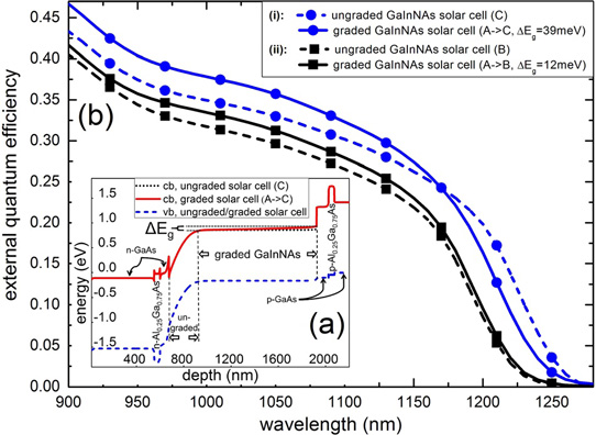
Figure 2: (a) Band lineup of pin-GaInNAs solar cells. (b) EQE measurements of GaInNAs solar cells with compositionally graded and ungraded GaInNAs layers.
The p- and n-type regions were GaAs. The 500nm n-GaAs cap was heavily doped to 5x10¹⁷/cm2 density. The p-type doping was 1x10¹⁷/cm2. The undoped GaInNAs region had p-type conductivity with a carrier density in the low 1016/cm2 range. The depletion layer between the n-GaAs and p-GaInNAs extended about 250nm into the ungraded part of the GaInNAs.
The fabricated cells had front contacts with 30μm-broad fingers and planar back contacts and mesa isolation of the p-i-n junction. The contact metal was annealed gold-germanium alloy.
The illumination source was a xenon lamp with about a one-third AM0 power density. The graded GaInNAs layers showed slightly degraded open-circuit voltage (VOC) (Table 2), attributed to the complex process resulting in more defects. Although the graded cells had higher short-circuit current density (JSC), the fill factor was lower due to the shifted absorption edge. The electric field induced from grading increased the external quantum efficiency (EQE) by 5% and 8% on average for A→B and A→C graded GaInNAs, respectively (Figure 2).
Table 2: Performance parameters under xenon lamp.
| GaInNAs layer | Open-circuit voltage | Short-circuit current density | Fill factor |
| A→C | 0.40V | 3.71mA/cm2 | 63% |
| A→B | 0.39V | 3.21mA/cm2 | 60% |
| C | 0.42V | 3.51mA/cm2 | 65% |
| B | 0.42V | 3.05mA/cm2 | 63% |
The researchers conclude: "We believe that it should, in principle, be possible to solve the trade-off between the increased JSC and the decreased VOC by further optimizing the growth process of the graded material to increase its crystal quality. Our initial results show that a material grading can in principle help to improve the charge carrier extraction in a GaInNAs solar cell. However, an optimized layout of a GaInNAs solar cell has to be carefully chosen and the material gradient might only be one feature among others (e.g. doping gradient, broad depletion width) promoting the current generation."
Multi-junction solar cells GaInNAs MBE GaAs substrates
http://dx.doi.org/10.1063/1.4922279
The author Mike Cooke is a freelance technology journalist who has worked in the semiconductor and advanced technology sectors since 1997.


