


- News
24 June 2015
Creating heterojunctions between black phosphorous and gallium arsenide
Researchers based in Germany and Switzerland have been studying the p-n diode properties of heterojunctions of thin-layer black phosphorous and gallium arsenide (GaAs) [Pascal Gehring et al, Appl. Phys. Lett., vol106, p233110, 2015].
Monolayer black phosphorous (phosphorene) has recently joined the ranks of two-dimensional electronic materials such as graphene and transition-metal dichalcogenides (TMDCs) as potential components of future ultra-small electronics.
Phosphorene tends to have p-type conductivity and has previously been combined with n-type molybdenum disulfide (MoS2) to create p-n junctions with sizable photo-response. Theoretical studies suggest bilayer phosphorene could be used for solar energy harvesting through photovoltaic effects with an external quantum efficiency (EQE) of up to 18%.
The team from Max Planck Institute for Solid State Research in Germany and Ecole Polytechnique Federale de Lausanne in Switzerland used heavily tellurium-doped n+-GaAs substrates with gold-germanium-nickel (AuGeNi) ohmic contacts. The substrate was thermally annealed to diffuse and alloy the contact metals into the GaAs substrate.
Thin flakes of 'phosphorene' were exfoliated from bulk black phosphorous crystal onto the suitably cleaned substrate, using the Scotch tape method frequently employed for graphene. The flakes had lateral diameters of up to several microns and the thickness was as low as 10nm. The conductivity of the flakes was found to be p-type – i.e. the carriers are holes. The level of p-type conductivity varies with thickness.
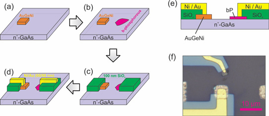
Figure 1: (a)-(d) Schematic representation of fabrication steps for thin-layer black phosphorous/GaAs p-n heterojunction devices. (e) Sketch of cross-section of completed device, and (f) optical micrograph of heterojunction device (top view).
A 100nm silicon dioxide film was deposited at the contact regions to avoid trivial Schottky contacts being formed between the phosporene contacts and the substrate. Nickel-gold was used as the phosphorene contact and as electrode to the nearest AuGeNi GaAs contact (Figure 1).
The device was protected from ambient degradation with a 50nm spin-on layer of poly(methyl methacrylate) (PMMA) thermoplastic.
The devices were rectifying, with the rectification ratio/asymmetry of the currents at +1V/-1V ranging between 100 and 1000. The large range is attributed to the varying areas and thicknesses of the flakes.
The low-bias ideality factor of 2 is said to be typical of theoretical diodes where the main mechanism of rectification is recombination current at the junction. At higher biases, the ideality factor increased. A device with 120 asymmetry had an ideality of 9.7 at 0.8V.
The researchers comment: "Such a high value indicates strong recombination due to defects, which might comprise intrinsic point defects inside the black phosphorous, surface defects on it arising from chemical degradation, or due to a bad contact between black phosphorous and GaAs. Another explanation involves the presence of an alternative transport channel (shunt resistance)."
Increased diffusion current above 0.8V caused the ideality to fall.
The photocurrent at zero bias of one device was measured under various laser wavelengths and powers (Figure 2). Under 514nm light, responsivity in the linear region was 37mA/W – the researchers say this is comparable with values for black phosphorous or carbon nanotubes on molybdenum disulfide heterojunctions under "sizable bias". The response flattened above 30μW to about 1.1μA "owing to the saturated optical absorption of the black phosphorous flake at high light intensities".
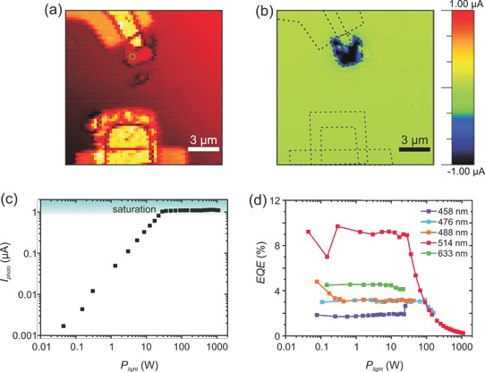
Figure 2: (a) Optical reflection image and (b) photocurrent map of device in Figure 1(f), recorded at zero source–drain bias. (c) Photocurrent as a function of laser power at 514nm wavelength. The signal was acquired from the green circle in panel (a). The blue-shaded region indicates current saturation. (d) EQE as a function of laser power for different laser light wavelengths.
The researchers comment: "In the present device, due to the very high doping level of the GaAs, the space-charge region is mostly confined to the black phosphorous layer, whereas only a very thin positive space-charge region exists in GaAs. Hence, the magnitude of the photocurrent is mainly governed by the number of available charge carriers inside the black phosphorous flake. Another reason is screening by the photo-generated carriers, which eliminates the bias across the depletion layer."
The 514nm wavelength gave the best zero-bias external quantum efficiency of 9.7% – "the same order of magnitude as reported for atomically thin TMDC heterostructures," according to the researchers. The enhanced performance at 514nm is attributed to van Hove singularities in the joint density of states.
The EQE under bias had a maximum of up to 31% with -2.5V reverse bias under 8.6μW 514nm wavelength over the range of devices produced.
The researchers also studied the photovoltaic performance under 514nm laser light. The maximum open-circuit voltage was ~0.6V, close to that estimated from the black phosphorous 0.56eV bandgap for a 15nm thick sheet. The maximum fill factor was ~0.3. Conventional solar cells reach 0.5-0.8. The researchers blame a low shunt resistance (leakage) and high series resistance. The high series resistance is thought to be due to high contact resistance of the black phosphorous and nickel/gold electrode. Lower values of contact resistance have been achieved on black phosphorous by other groups.
The photo-conversion efficiency – the ratio of electric power output to light power input – was measured with a maximum of 0.24%, again comparable with black phosphorous on MoS2.
The researchers believe that improved performance would result from "better control of the chemical nature of the black phosphorous surface, complemented by the implementation of improved electrical contacts".
Monolayer black phosphorous GaAs GaAs substrates p-n heterojunction
http://dx.doi.org/10.1063/1.4922531
The author Mike Cooke is a freelance technology journalist who has worked in the semiconductor and advanced technology sectors since 1997.


