


- News
23 June 2015
Long-wavelength N-polar indium gallium nitride LEDs
Researchers in Japan have been developing long-wavelength N-polar indium gallium nitride (InGaN) light-emitting diodes (LEDs) [Kanako Shojiki et al, Appl. Phys. Express, vol8, p061005, 2015]. By varying the metal-organic vapor phase epitaxy (MOVPE) growth temperature between 880°C and 790°C, the emission wavelength was changed from 444nm to 633nm.
In making longer-wavelength devices, InGaN with high indium content is needed. The researchers from Tohoku University and the CREST funding program of the Japan Science and Technology Agency studied −c-plane/N-polar MOVPE since indium incorporation is more efficient than for +c-plane/Ga-polar growth. However, −c-plane MOVPE growth is more difficult to achieve and growth conditions need more strict optimization.
One problem with high-indium-content InGaN alloy is that that the InN and GaN components do not mix uniformly (phase separation).
The team used a horizontal reactor for metal-organic vapor phase epitaxy on c-plane sapphire. The substrate was off-cut at 0.8° around the a-axis, a smaller angle than previous research on −c growth by University of California Santa Barbara (UCSB) in the USA. The researchers believed that the smaller angle would reduce step-bunching in the growth.
N-polar growth was initiated with a nitridation step. A buffer of −c-plane 1μm GaN was followed by 1.8μm of n-type GaN. Both these layers were grown at 1100°C.
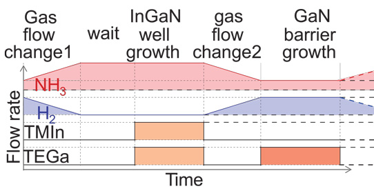
Figure 1: Schematic for one-period sequences of gas flow of InGaN/GaN MQW.
Five InGaN wells were grown in GaN barriers. The wells and barriers were grown with different gas mixture ratios (Figure 1). Hydrogen carrier gas was not used in the InGaN growth steps. Hydrogen inhibits indium incorporation.
The structure was capped off with p-GaN grown at 930°C. For the LEDs, the n- and p-type electrodes were titanium/aluminium/titanium/gold and nickel/gold, respectively. The current injection area was 67,600μm2
The growth of the multiple quantum well (MQW) active region was carried out at six different temperatures between 790 and 880°C. X-ray analysis of the wells showed no strain relaxation, in contrast to long-wavelength LED materials produced in the +c-direction by Tokyo University of Science.
The electroluminescence (EL) spectra blue-shifted to shorter wavelengths with increased current – an effect attributed to screening of the quantum-confined Stark effect and band filling, as seen in +c-plane devices. For an LED with 810°C MQW, the shift was 47nm between 5.3A/cm2 and 137.6A/cm2. The peak was around 600nm (orange). Self-heating effects reduced the efficiency at high current injection, associated with the low hole concentration in the p-GaN layer and increased non-radiative recombination.
Transmission electron microscopy (TEM) and x-ray diffraction (XRD) analysis gave estimates for the InGaN well thickness of 2.8nm and GaN barrier thickness of 8.7nm. The indium composition of the wells was 21%. For +c-plane wells with the same indium composition, the peak wavelength is generally around 100nm shorter. The researchers comment: "This means that −c-plane LEDs have a higher density of localized emission centers associated with a high-indium-content and/or a thick region, which cannot be detected by XRD."
One expects in both −c- and +c-plane growth similar amounts of phase separation, leading to high-indium-content regions. However, at the present stage, the thickness uniformity of −c-plane deposition is inferior to the more established +c-plane processes.
Table 1: EL characterization of −c-plane InGaN LEDs with MQW temperatures ranging from 790°C to 880°C.
| Tg,MQW | 790°C | 810°C | 820°C | 830°C | 850°C | 880°C |
| Injection current | 20mA (29A/cm2) | 20mA (29A/cm2) | 20mA (29A/cm2) | 20mA (29A/cm2) | 20mA (29A/cm2) | 80mA |
| EL peak wavelength | 633.4nm | 600.5nm | 551.0nm | 506.8nm | 488.6nm | 444.4nm |
| EL intensity | 0.7mW/cm2 | 1.9mW/cm2 | 14.0mW/cm2 | 32.5mW/cm2 | 10.7mW/cm2 | 0.3mW/cm2 |
The effect of increasing MQW growth temperature was to shorten the peak EL wavelength (Table 1). The researchers claim that their 633.4nm LED with 790°C MQW had a longer wavelength than previously reported −c-plane devices. In particular, this wavelength was 85nm longer than a reported −c-plane LED produced using plasma-assisted molecular beam epitaxy (PAMBE).
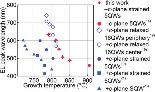
Figure 2: Dependence of EL peak wavelength and Tg,MQW of +c-plane and −c-plane LEDs under driving current of 20mA.
The researchers comment: "A comparison among the LEDs on sapphire substrates grown by the same growth method of MOVPE reveals that the output power and maximum EL peak wavelength of our LEDs far exceeded those previously reported for −c-plane LEDs."
InGaN LEDs LEDs InGaN GaN MOVPE
http://dx.doi.org/10.7567/APEX.8.061005
The author Mike Cooke is a freelance technology journalist who has worked in the semiconductor and advanced technology sectors since 1997.


