


- News
16 March 2015
EVG adds two EVG580 ComBond system configurations for university/R&D and high-volume manufacturing
EV Group (EVG) of St Florian, Austria (a supplier of wafer bonding and lithography equipment for MEMS, nanotechnology and semiconductor applications) has introduced two new configurations to its EVG580 ComBond series of automated high-vacuum covalent wafer bonding systems. Addressing the needs of universities and R&D institutes, and high-volume manufacturing (HVM) requirements, respectively, both system configurations achieve electrically conductive and oxide-free bonds of materials with different lattice constants and coefficients of thermal expansion at room temperature.
Applications that demand room-temperature bonding of substrates with very different material properties and that are supported by the EVG580 ComBond series include engineered substrates, power devices, stacked solar cells and emerging technologies such as silicon photonics.
The new entry-level EVG580 ComBond system for universities and R&D institutes comes with one cassette station or manual load port as well as a single-arm robot, supporting up to three process modules.
The EVG580 ComBond HVM system can be configured with two cassette stations or an equipment front-end module with up to four cassettes for continuous mode operation, as well as comes with a dual-arm robot to support up to six process modules for maximum throughput.
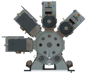 Picture: Top view of an EVG580 ComBond automated high-vacuum wafer bonding system. The integrated cluster system enables fully automated wafer transport, handling and processing in high vacuum.
Both new ComBond system configurations, as well as the standard system that can accommodate up to five process modules, are built on a modular platform supporting wafers up to 200mm in diameter. In addition to one or more bond chambers, the systems feature a dedicated ComBond Activation Module (CAM), which provides advanced surface preparation by directing energized particles to the substrate surface to achieve a contamination-free and oxide-free bond interface. The systems operate in a high-vacuum-process environment with base pressures in the range of 5x10⁻⁸mbar, which prevents re-oxidation of the treated wafers prior to the bonding step.
"The EVG580 ComBond system with its standard five-module configuration, which was launched last autumn, has already demonstrated its capabilities with multiple R&D partners and customers," says EVG's corporate product management director Dr Thomas Glinsner. "With the new three-module system, we will now make this breakthrough technology available to universities and smaller R&D institutes, which often are at the forefront of pioneering advanced electronic materials and device research, such as heterogeneous integration of compound semiconductors for silicon photonics and other leading-edge applications," he adds. "All ComBond systems can be further customized to address specific application development needs, such as with special metrology modules utilizing free ports of the high-vacuum handling."
EVG unveils covalent bonder for engineered substrate and power device production
www.evgroup.com/ComBond_ShortBrochure.pdf


