


- News
16 March 2015
GaN Systems' power semiconductors gain top-side cooling for simpler PCB design
GaN Systems Inc of Ottawa, Ontario, Canada, a fabless producer of gallium nitride (GaN)-based power switching transistors based on its proprietary Island Technology for power conversion and control applications, has announced new top-side cooling technology in its range of high-power enhancement-mode devices.
Top-side cooling enables the use of conventional, well-understood PCB cooling techniques when incorporating the firm's devices into the latest designs for products such as inverters, uninterruptible power supplies (UPS), hybrid electric vehicles/electric vehicles (HEV/EV), high-voltage DC-DC conversion, and consumer products such as TVs.
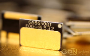
GaN Systems' gallium nitride power transistors are based on its proprietary Island Technology - the die consist of islands rather than traditional fingers, which brings advantages in terms of better current handling, lower inductance, scaling, isolation and thermal management, as well as enabling smaller die and lowering cost, it is claimed. With current ratings ranging from 8A to 250A, the firm's enhancement-mode devices are delivered in its proprietary GaNPX packaging: the die is embedded within a laminate construction and a series of galvanic processes replaces conventional techniques such as clips, wire bonds and moulding compounds. These near-chipscale high-power switching transistors are now packaged to be cooled via the top-side of the chip using a heat-sink or fan – conventional techniques that are well-understood and familiar to design engineers who may be unfamiliar with using GaN devices or using them for the first time, the firm says.
 GaN transistors can also be cooled from the bottom surface of the die through conduction to the PCB.
GaN Systems says that it is the first company to have developed and brought to the global market a comprehensive range of devices with current ratings from 8A to 250A – its Island Technology die design, combined with its extremely low inductance and thermally efficient GaNPX packaging and Drive Assist technology means that the firm's GaN transistors offer a 40-fold improvement in switching and conduction performance over traditional silicon MOSFETs and IGBTs, it is claimed.
'Wide bandgap semiconductor devices in power electronics – Who, What, Where, When and Why?' panel discussion at APEC
At the 30th IEEE Applied Power Electronics Conference and Exposition (APEC 2015) in Charlotte, NC, USA (17 March, 5–6.30pm), GaN Systems is participating in a panel discussion on the topic 'Wide Bandgap Semiconductors devices in Power Electronics – Who, What, Where, When and Why?', hosted and led by Kevin Parmeter, VP applications at Excelsys Technologies joined by panellists from device manufacturers and power electronics design engineers.
GaN Systems' VP sales & marketing Larry Spaziani is joining representatives from Rompower, Efficient Power Conversion Corp, Excelsys Technologies, IR/Infineon, Embedded Power Labs and Vishay to discuss questions such as: "Are we on the verge of a revolution that is taking place now, or is this something that will be become mainstream in five, ten or even twenty years?", "What are the technical hurdles and packaging constraints?", and "Who will the players be?".


