


- News
11 March 2015
Hole modulation for increased light output power from InGaN LEDs
Researchers based at Singapore's Nanyang Technological University and Turkey's Bilkent University have developed 'hole modulation' structures to improve hole injection into indium gallium nitride (InGaN) multiple quantum well (MQW) light-emitting diodes (LEDs) [Zi-Hui Zhang et al, Appl. Phys. Lett., vol106, p063501, 2015].
Hole injection in InGaN LEDs is adversely affected by two factors: the poor doping efficiency of magnesium and the use of aluminium gallium nitride (AlGaN) electron-blocking layers (EBLs). Poor doping efficiency leads to low hole density in p-GaN layers. The problem with EBLs is that, while they raise a barrier against electron overflow (increasing confinement of electrons in the MQW active light emitting region), they also present a block to hole injection into the MQW.
The NTU/Bilkent technique is to partially dope the last barrier of the MQW with magnesium. The effect is to accumulate holes in the p-GaN contact layer near the EBL and to reduce the EBL barrier. The researchers report a 25.6% increase in light output power at 80A/cm2 injection current density. The EBL barrier to hole injection was estimated to be 294meV, compared with 332meV for structures without last-barrier doping.
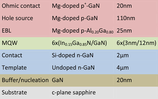
Figure 1: Epitaxial structure of LEDs.
The epitaxial structures (Figure 1) were grown by metal-organic chemical vapor deposition (MOCVD) on c-plane sapphire. The last 12nm GaN barrier of the multiple quantum well structure was either undoped (LED A) or doped with magnesium in the last 6nm of growth (LED B). The structures were anneal in-situ at 720°C for 600 seconds in nitrogen to activated the p-type magnesium doping.
The researchers performed simulations that suggested the doped last barrier would act as a 'hole modulator'. In the unbiased state (Figure 2), holes from the last barrier are depleted by the built-in electric field from charge polarization effects due to the partially ionic character of the chemical bonds in III-N compound semiconductors like GaN.
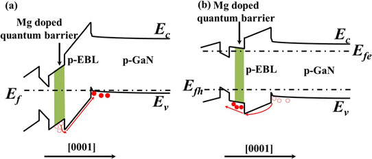
Figure 2: Schematic energy band diagrams for InGaN/GaN MQWs, p-EBL, and p-GaN: (a) under no bias, last quantum barrier is partially p-type doped (indicated by shadow region), (b) under bias, the holes will then be injected into MQWs. Ec, Ev, Ef, Efe and Efh denote the conduction band, valance band, Fermi level, quasi-Fermi levels for electrons, and holes, respectively.
These holes accumulate in the p-GaN on the other side of the AlGaN electron-blocking layer. The hole accumulation is in a thin two-dimensional layer due to the charge-polarization-induced negative charges at the EBL/p-GaN interface.
Under bias, these holes are more easily injected into the MQW active region, compared with LED A without doping in the last barrier. Experimental determination of the hole concentration profile with capacitance-voltage measurements confirmed the picture derived from the simulations (with 'slight discrepancies').
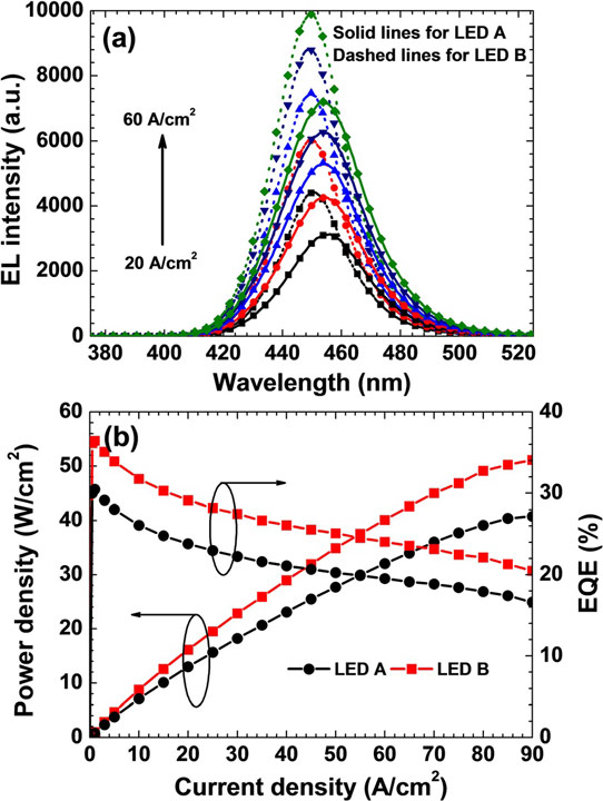
Figure 3: Experimentally measured (a) EL spectra at 20A/cm2, 30A/cm2, 40A/cm2, 50A/cm2 and 60A/cm2, solid lines and dashed lines are for LED A and LED B, respectively, and (b) optical output power density and external quantum efficiency for LEDs A and B, respectively.
Test LED 1mmx1mm dies were produced from the two epitaxial structures with indium bump ohmic contacts. The peak emission wavelength for LED A electroluminescence (EL) was at 454nm – LED B produced a shorter wavelength of 450nm (Figure 3). The difference was attributed to fluctuations in the conditions between the two growth runs. LED B produced stronger emission than LED A under all current density levels. At 80A/cm2, the power output of LED B was 25.6% greater than for LED A.
LED B also shows improved external quantum efficiency (EQE) up to 90A/cm2. The presented graph cuts off at the point where the EQE peaks (for both LEDs) and one would expect the usual droop effect beyond this, although this is not mentioned in the paper.
LEDs InGaN LEDs InGaN GaN MOCVD
http://dx.doi.org/10.1063/1.4908118
The author Mike Cooke is a freelance technology journalist who has worked in the semiconductor and advanced technology sectors since 1997.


