


- News
4 March 2015
Silver nanowires and gallium nitride increase efficiency of Schottky UV-LEDs
Zhejiang University in China and University of Cambridge in the UK have jointly developed ultraviolet light-emitting diodes (UV-LEDs) based on metal-semiconductor Schottky junctions between silver nanowires (AgNWs) and gallium nitride (GaN) [Y. Wu et al, Appl. Phys. Lett., vol106, p051108, 2015].
The external quantum efficiency (EQE) for radiation around a wavelength of 362.5nm was as high as 0.9%. The researchers comment: "The EQE of our device is the highest reported to date for UV LEDs based on a Schottky junction."
UV-LEDs are being developed for a wide range of applications such as high-density information storage, water purification, disinfection of medical tools, UV curing, phototherapy, and medical diagnostics.
The researchers see three advantages of Schottky-type LEDs (ST-LEDs) over conventional multiple quantum well (MQW) devices: "First, ST-LEDs do not require complex processing such as those required for MQWs. Second, the device operation does not rely on a p-n junction, reducing the difficulties associated with doping of semiconductors. Finally, it does not require deliberate introduction of an intrinsic layer to reduce leakage current and to accumulate carriers near the interface, a key process in [metal-insulator-semiconductor] MIS LEDs."
Conventional ST-LEDs suffer a tradeoff from the metal layer absorbing a significant percentage of the LED output, reducing overall efficiency. The use of nanowires reduces this blocking of radiation.
The Zhejiang/Cambridge devices have a simple structure (Figure 1) that the researchers believe has "the potential to be a cost-effective alternative to traditional UV-LEDs and can also be integrated into nano-optoelectronic systems".
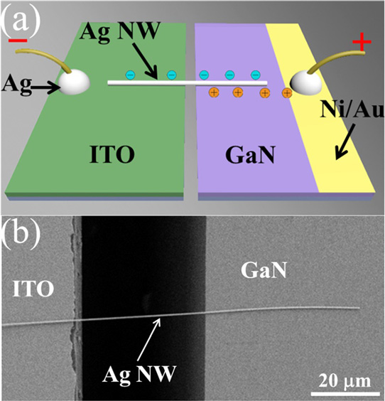
Figure 1: (a) Schematic of the single Ag NW/p-GaN ST-LED. (b) SEM image of the as-fabricated device.
The semiconductor material for the device was p-type gallium nitride (p-GaN) grown on sapphire by metal-organic chemical vapor deposition (MOCVD). The diode fabrication began with cleaning and etching to remove native oxide from the GaN surface. After rinsing and drying, the nickel/gold p-electrode (anode/p-contact) was deposited by thermal evaporation. The cathode (n-contact) was an indium tin oxide (ITO)-covered sapphire substrate micro-manipulated to give a gap of less than 0.35μm from the GaN substrate.
The gap between the p-GaN and ITO was bridged by silver nanowires produced by 'soft self-seeding'. The nanowires were produced from silver nitrate reduced with ethylene glycol (EG) in the presence of polyvinyl pyrrolidone (PVP). The resulting wires were 120-500nm diameter and more than 50μm long. The nanowires were purified in several cycles by immersing in ethanol, centrifuging and then rinsing in deionized water.
The nanowire suspension was deposited on clean glass. Single nanowires were then transferred to bridge the gap between the ITO and GaN substrates. The AgNWs were held in place by van der Waals forces.
The current-voltage curve of the device was rectifying with a forward bias onset at 4.8V (Figure 2). The silver-ITO and GaN-nickel/gold contacts were found to be ohmic in separate tests. The diode behavior was therefore a result of the Ag/p-GaN contact.
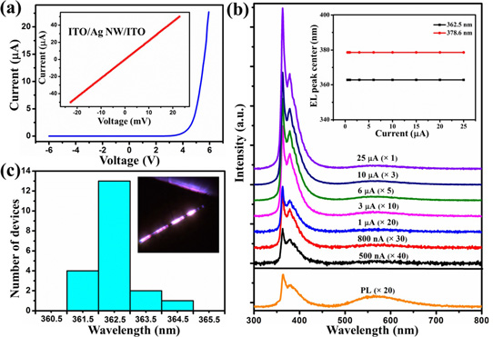
Figure 2: (a) Current versus voltage (I-V) characteristics of as-fabricated device. Inset: ohmic contact behavior of ITO/Ag NW/ITO structure. (b) EL spectra of device under various injection currents and the photoluminescence (PL) spectrum of p-GaN under 355nm pulsed laser excitation. Inset: EL peak position (362.5nm and 378.6nm) versus different forward currents of same device. (c) Dominant emission peak distribution of 20 devices. Inset: a typical optical microscope image of emission.
Electroluminscence (EL) was observed for forward currents as low as 500nA. The UV emission included two contributions – a main peak at 362.5nm with 7nm full-width at half maximum (FWHM) and a second peak at 378.6nm with 30nm FWHM.
The researchers attribute the main peak to recombination through an exciton state (electron-hole bound state). The second peak was assigned to isolated magnesium atoms from the p-GaN doping. There was also weaker defect-related emission from the visible range 480-710nm.
Much of the emission was trapped in the GaN because of total internal reflection from the GaN/air interface. The trapped light is emitted from the edge of the device. The light output intensity increased as a 1.24 power of the current injection. The 'superlinear' behavior of the intensity is attributed to the changing balance of radiative and non-radiative recombination mechanisms. At 25μA injection the external quantum efficiency was estimated at 0.9%.
The team attributes the relatively high efficiency to the reduced blocking of the light by the nanowires compared with the usual metal electrodes. "The performance is also comparable to those of UV-LEDs based on NW/thin-film p-n hetero/homo-junctions and MIS junctions, with a simpler device architecture and potentially lower fabrication cost," the researchers add.
The highest efficiency was obtained for nanowires of 250nm diameter. Beyond that, self-heating effects reduced the performance to 70% of the maximum EQE with 170nm diameter. (The current injection was not pulsed to avoid self-heating effects.) Narrower wires are less able to transmit heat away from the AgNW/GaN junction.
Schottky UV-LEDs UV-LEDs Silver nanowires GaN GaN substrates MOCVD
http://dx.doi.org/10.1063/1.4907568
The author Mike Cooke is a freelance technology journalist who has worked in the semiconductor and advanced technology sectors since 1997.


