


- News
20 May 2015
Gallium nitride HEMT-LED without metal interconnection
Hong Kong University of Science and Technology (HKUST) has produced indium gallium nitride (InGaN) light-emitting diodes directly connected with aluminium gallium nitride (AlGaN) barrier high-electron-mobility transistors (HEMTs) [Chao Liu et al, Appl. Phys. Lett., vol106, p181110, 2015].
The researchers comment: "We believe the demonstrated integration scheme of the HEMT-LED is highly promising for a wide range of applications, such as smart lighting, displays, and optical communications."
The production of HEMT-LEDs without metal interconnections (Figure 1) reduces the influence of parasitic losses in terms of power and time delay. However, combining InGaN and AlGaN processing can be tricky.
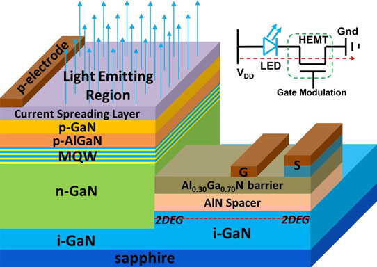
Figure 1: Schematic of finished HEMT-LED device. Inset: equivalent circuit diagram of device.
The Hong Kong team first grew the layers for the HEMT on sapphire using metal-organic chemical vapor deposition (MOCVD). The sequence was 3.0μm GaN buffer, 100nm GaN channel, 1nm AlN spacer, and 20nm AlGaN barrier. The channel layer was grown at higher pressure and III/V ratio than the buffer to improve the mobility of the two-dimensional electron gas (2DEG) conducting region. The Hall mobility was 1530cm2/V-s with a carrier density of 1.2x10¹³/cm2. The sheet resistance was 330Ω/square.
The LED layers were re-grown on the GaN buffer layer selectively exposed with inductively coupled plasma etch using a silicon dioxide mask. The n-GaN contact layer of the LED was 1.6μm. The active region was a 5-period InGaN/GaN multiple quantum well with 3nm wells and 11nm barriers. The p-contact layers consisted of 15nm p-Al0.15Ga0.85N for electron blocking, and 170nm p-GaN.
The LED 450μmx460μm mesa was fabricated using ICP etch with the HEMT region protected by photoresist. The HEMT mesa was similarly produced with the LED region protected. The annealed ohmic source electrode was titanium/aluminium/nickel/gold. The p-contact of the LED consisted of a nickel/gold current spreading layer and titanium/aluminium/titanium/gold electrode. The Schottky gate for the HEMT was nickel/gold.
Scanning electron microscopy (SEM) showed that the channel of the HEMT was in "intimate contact" with the n-type layer of the LED, giving a three-terminal LED-HEMT. The researchers estimate that the interconnection resistance was reduced by an order of magnitude compared with devices connected with wires.
The team comments: "The reduced parasitic resistance accounts for approximately 15% of the total parasitic resistance of the driving circuit, which can help cut down the delay time (RC) of the driving circuit." Parasitic inductance and resistance also increase power consumption, generating heat and lowering efficiency. Other potential advantages over metal wire interconnection include smaller footprint, reduced fabrication complexity, and enhanced device reliability.
The researchers have previously tried to produce HEMTs after the material for the LED has been grown. This resulted in a 1mA/mm off-state breakdown at 40.5V. By contrast, the HEMT-first approach resulted in a reduction in off-current by three orders of magnitude, with an off-current of 6.3μA/mm at 200V. The researchers attribute the difference to the high resistance of the buffer being maintained in the HEMT-first method, even after the high-temperature selective growth process for the LED layers.
A single HEMT produced on sapphire had a maximum drain current of 420mA/mm and 12.8Ω-mm on-resistance. The performance of a HEMT-first LED-HEMT had similar performance except for a shift of 3V in potential difference from the drain bias of the HEMT-only device. This was due to the turn-on voltage of the LED. At high bias, the LED resistance of 11Ω was negligible compared with the on-resistance of the HEMT of 128Ω.
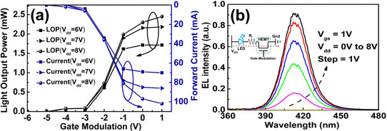
Figure 2: (a) LOP and current-voltage characteristics of fabricated HEMT-LED device modulated by gate biases at different drain voltages and (b) electroluminescence spectrum modulated by drain bias at 1V gate.
The light output power (LOP) was controlled by both the gate potential and the bias across the LED-HEMT (Figure 2)
InGaN LED AlGaN barrier HEMT MOCVD
http://dx.doi.org/10.1063/1.4921049
The author Mike Cooke is a freelance technology journalist who has worked in the semiconductor and advanced technology sectors since 1997.


