


- News
6 May 2015
Reducing on-resistance in vertical gallium nitride MOSFETs
Toyoda Gosei Co Ltd in Japan has developed a vertical trench metal-oxide-semiconductor field-effect transistor (MOSFET) on free-standing gallium nitride (GaN) combining 1.2kV blocking voltage with low specific on-resistance [Tohru Oka et al, Appl. Phys. Express, vol8, p054101, 2015]. The researchers comment: "To the best of our knowledge, this is the first report on vertical GaN-based MOSFETs with a specific on-resistance of less than 2mΩ-cm2."
The threshold voltage was +3.5V, which is high compared with the values usually achieved with lateral structure GaN-based devices. High-power automotive applications need normally-off devices with thresholds above 3-5V to prevent false switching arising from noise and other factors. The advantage of lateral devices is lower specific on-resistance in general. A vertical structure should allow the reduction of chip size and production cost reduction.
Toyoda Gosei mainly supplies plastic and rubber parts to the automotive industry, along with white LEDs and general industrial products. The company's white LEDs will be manufactured using GaN technologies. Toyoda Gosei says that its main LED applications are tablet computers and liquid-crystal displays, although it also produces various other lighting devices that use LEDs, including fluorescent and security lights.
Metal-organic chemical vapor deposition (MOCVD) was used to create the epitaxial structure for the vertical transistors on free-standing n+-GaN substrates with 0.2μm n+-GaN, 0.7μm p-GaN, and 13μm n--GaN. The 13μm drift layer was thinner, but more heavily doped, than the group's previous devices. The thinner layer was designed to reduce resistance, while maintaining 1.2kV-class blocking voltage. The p-GaN channel was also thinned, and the doping concentration reduced. The aim, here, was also to reduce resistance.
Transistor fabrication (Figure 1) involved inductively couple plasma (ICP) etching for mesa isolation, p-body contact recessing, and gate trenching. The gate dielectric was 80nm silicon dioxide, grown using atomic layer deposition (ALD). Interlayer dielectrics of 100nm aluminium oxide and 800nm silicon dioxide were produced by atomic layer deposition and plasma-enhanced chemical vapor deposition (PECVD).
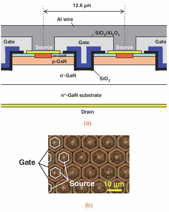
Figure 1: MOSFET schematic (a) and micrograph of hexagonal transistor array.
The p-body electrode was palladium; the source/drain electrodes were titanium/aluminium. The source electrode was stacked on top of the p-body electrode to reduce the cell pitch (12.6μm). The device was annealed at 550°C for 5 minutes in nitrogen to produce ohmic contacts.
Potential crowding at the pn-junction edge was reduced with field-plate termination around the isolation mesa periphery.
The transistors were produced in an array with a hexagonal trench gate layout. The researchers write that there is a definite advantage of polygonal cells over striped devices in terms of channel density, increasing the ratio of gate width to unit cell area (0.267/μm) by a factor of two over a stripe-cell device (15μm pitch). This should reduce specific on-resistance.
The MOSFET achieved 0V off-state blocking up to 1250V. At +40V gate potential the current density was 10.2mA/mm with a 0.5V drain bias. The researchers comment that this is 3.3x the value obtained in their previous devices with the same gate potential.
The forward-sweep threshold voltage was +3.5V. The team observes that theoretical considerations would lead one to expect a threshold of 33V. The significant difference is attributed tentatively to the presence of fixed charges at the interface between the gate dielectric and trench surface. There was also hysteresis of 0.5V in the backward-sweep threshold.
The linear region with a gate potential of 40V demonstrated a specific on-resistance of 1.8mΩ-cm2 (Figure 2), which is a 6.6-fold reduction on the group's previous work. The improvement is attributed to the increased ratio of gate width to unit cell area (2x) and current density per unit gate length (3.3x). These improvements were based on the hexagonal layout and an enhanced epitaxial process.
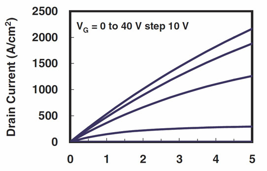
Figure 2: Drain current versus voltage for range of gate potentials.
The researchers comment: "The results demonstrated that the performance of vertical GaN MOSFETs is approaching the best performance of SiC MOSFETs." The team believes that further miniaturization could lead to sub-1mΩ-cm2 specific on-resistance 1.2kV-class devices.
Toyoda Gosei GaN MOSFET Free standing GaN MOCVD ALD
http://dx.doi.org/10.7567/APEX.8.054101
The author Mike Cooke is a freelance technology journalist who has worked in the semiconductor and advanced technology sectors since 1997.


