


- News
27 May 2015
Metal-insulator-semiconductor gated hybrid anode GaN-on-Si diode
University of Electronic Science and Technology of China has developed a gallium nitride-on-silicon (GaN-on-Si) metal-insulator-semiconductor gated hybrid anode diode (MG-HAD) with low onset voltage, on-resistance and reverse current leakage [Qi Zhou et al, IEEE Electron Device Letters, published online 12 May 2015]. Breakdown voltages of more than 1.1kV were achieved with a 10μA/mm criterion.
The MG-HAD consisted of a hybrid anode with electrically shorted ohmic and recessed metal/aluminium oxide/III-nitride MIS gate. The threshold voltage was determined by the degree of depletion of the two-dimensional electron gas (2DEG) channel beneath the gate region – this could be modulated by modifying the recess depth.
Although better performance has been achieved with GaN diode devices, this has been at the cost of using more expensive, smaller-diameter substrates such as free-standing GaN, silicon carbide, or sapphire. A further attraction of GaN-on-Si is the potential for integration with conventional silicon CMOS electronics.
The researchers used a commercial heterostructure material from Enkris Semiconductor (www.enkris.com) that consisted of 4-inch silicon (111) substrate, 3.5μm GaN buffer, 1nm AlN spacer, 23nm Al0.23Ga0.77N barrier, and 2nm GaN cap. The carrier density and mobility in the 2DEG were 9.5x10¹²/cm2 and 1500cm2/V-s, respectively.
Device fabrication (Figure 1) began with 100nm silicon nitride passivation, reactive ion etch to open the ohmic regions, native oxide removal, and titanium/aluminium/nickel/gold ohmic metal deposition.
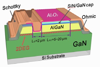 Figure 1: Schematic three-dimensional device structure of MG-HAD. Gate length and overhanging extension were 2μm and 0.5μm, respectively. Gate width was 50μm.
Further etching removed silicon nitride in the gated region, created mesa isolation, and cut through the GaN cap and 16nm of the AlGaN barrier. The etching was completed with a low-damage digital oxygen plasma etch process and hydrochloric acid rinse to remove native oxide. The 10-cycle digital etch removed some 5nm of material creating a recessed 2nm AlGaN barrier. The 2DEG under the recessed region was completely depleted.
The device was completed with 10nm aluminium oxide from atomic layer deposition (ALD) and annealing, and evaporation of nickel/gold Schottky metal.
Devices with 5μm anode-cathode distance (LAC) had a 1mA/mm forward current threshold of 0.6V, a 0.3V reduction compared with reference Schottky barrier diodes (SBDs) produced on the same substrate. The specific on-resistance of MG-HAD and SBD were 0.6mΩ-cm2 and 1.24mΩ-cm2, respectively. The researchers attribute the lower MG-HAD resistance to the current flow through the ohmic part of the anode contact.
The reverse current leakage was two orders of magnitude (1/100) lower for the MG-HAD, compared with the SBD reference. The team says this is due to the insertion of aluminium oxide insulation between the AlGaN barrier and recessed gate.
Varying LAC between 5μm and 20μm had little effect on the threshold, which had an average value of 0.66V with 0.07V standard deviation for 189 devices. This was due to the low-damage, controllable recessing, according to the researchers.
The researchers also compared the reverse current leakage and breakdown of the MG-HADs and SBDs. The team applied a more rigorous breakdown criterion for the MG-HAD of 10μA/mm, compared with the more usual 1mA/mm for the SBD. A 20μm LAC MG-HAD broke down at more than 1100V. The reverse voltage for 1μA/mm leakage was 790V, giving an on/off current ratio for the device of five orders of magnitude. Similarly dimensioned SBDs had 1mA/mm breakdowns at around 500V.
The MG-HAD breakdown was attributed to buffer leakage bypassing the 2DEG path between the ohmic cathode and anode. The researchers suggest that AlGaN back barriers or thicker low-dislocation-density buffers should increase the breakdown voltage.
Thermal measurements showed an increase of on-resistance with temperature by a factor of 1.9 between 25°C and 150°C. The breakdown voltage was 615V at 150°C.
A 10μm LAC MG-HAD had 10μA/mm breakdown (BV) at 857V with corresponding specific on-resistance (RON,SP) of 1.6mΩ-cm2. The BV2/RON,SP figure of merit was 459MV/cm2.
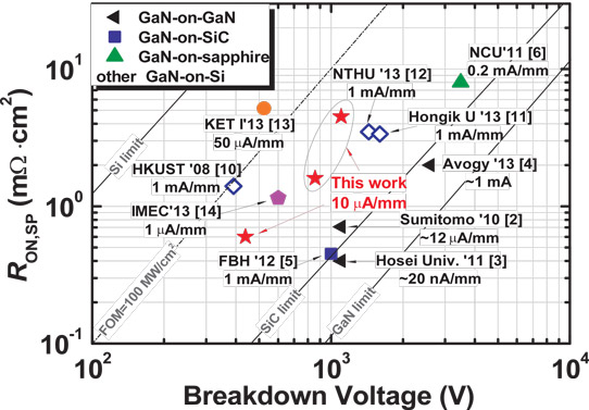
Figure 2: Benchmark of RON,SP versus BV of GaN power diode on GaN/SiC/sapphire/Si substrates.
The researchers comment on the comparison with other state-of-the-art devices (Figure 2) that "[the MG-HAD] value is among the best results reported for GaN-on-Si power diode at reverse leakage as low as 10μA/mm."
http://ieeexplore.ieee.org/xpl/articleDetails.jsp?arnumber=7105851
The author Mike Cooke is a freelance technology journalist who has worked in the semiconductor and advanced technology sectors since 1997.


