


- News
27 November 2015
Ultraviolet photodetectors on free-standing gallium nitride
Researchers based in USA have been studying performance improvements in aluminium gallium nitride (AlGaN) ultraviolet (UV) avalanche photodiodes (APDs) gained from using free-standing gallium nitride substrates instead of gallium nitride on sapphire templates [Jeomoh Kim et al,Appl. Phys. Express, vol8, p122202, 2015].
The work involved Georgia Institute of Technology, University of Houston, Magnolia Optical Technologies Inc, US Army Night Vision Sensors and Electronic Division, and the US Defense Advanced Research Projects Agency (DARPA) Microsystems Technology Office (MTO).
AlGaN-based photodetectors have potential for high optical gain, high sensitivity, low dark current and detection of solar-blind radiation. Alternative technologies are photomultiplier tubes and silicon (Si)-based photodetecting devices. Photomultpliers are bulky and fragile, while silicon is a less efficient detector of UV, given that it has an indirect bandgap. Silicon's narrower bandgap also means that it is sensitive to solar radiation.
Producing high-quality AlGaN material is a challenge to fabricating high-performance photodetectors. The researchers explain: "A high density of crystalline defects, mainly threading dislocations, of AlGaN layers in an active region results in high leakage current and premature microplasma breakdown prior to reaching avalanche breakdown."
The epitaxial material (Figure 1) was grown by metal-organic chemical vapor deposition (MOCVD) on free-standing GaN or GaN-on-sapphire. Where the aluminium content of the structure (n-contact region) changed, the researchers used step-grading strain management of the transitions to avoid cracking.
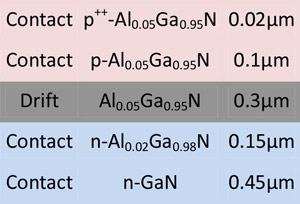 Figure 1: Epitaxial material structure for p-i-n APDs on free-standing GaN substrate or GaN/sapphire template.
The free-standing GaN substrate was n-type conductive, produced in a thick-film hydride vapor phase epitaxy (HVPE) process. The threading dislocation density was less than 5x10⁶/cm2.
The GaN-on-sapphire template was produced by creating a low-temperature GaN buffer and then growing 3μm unintentionally doped GaN. The resulting dislocation density was 5.4x10⁸/cm2, as determined by x-ray analysis.
The materials were fabricated into top-illuminated APDs with circular mesas. The annealed n- and p-contacts were titanium/aluminium/titanium/gold and nickel/silver/nickel/gold, respectively. The APDs were passivated with silicon dioxide. Interconnect and bond pads consisted of titanium/gold.
One effect of using free-standing GaN substrates was to increase the breakdown voltage under reverse bias to 95-100V, compared with 87-89V for the devices on GaN/sapphire templates. Also, the dark current was significantly reduced in APDs on free-standing GaN by factors ranging from 2x to 10x, depending on mesa diameter.
The researchers comment: "Considering the fact that dislocations in a device would increase the dark-current density by trap-assisted tunneling current at a certain reverse bias and produce premature micro-plasmas prior to the onset point of avalanche breakdown, the use of a FS-GaN substrate with a low dislocation density is responsible for the low dark-current density and constant breakdown voltage of UV-APDs."
The relatively small change in dark current with mesa size indicates that surface leakage through the mesa walls was small, according to the researchers. The team adds: "The low etch damage of the mesa definition and high-quality dielectric passivation during the fabrication process possibly contributed to reducing the leakage current through the mesa sidewall surfaces."
The researchers estimated the peak field in a 40μm-diameter APD (1256μm2 area) on free-standing GaN at ~3.2MV/cm in a one-dimensional simulation. This compares with the critical fields in GaN (2.4-3.3MV/cm) and Al0.22Ga0.78N (3.5MV/cm).
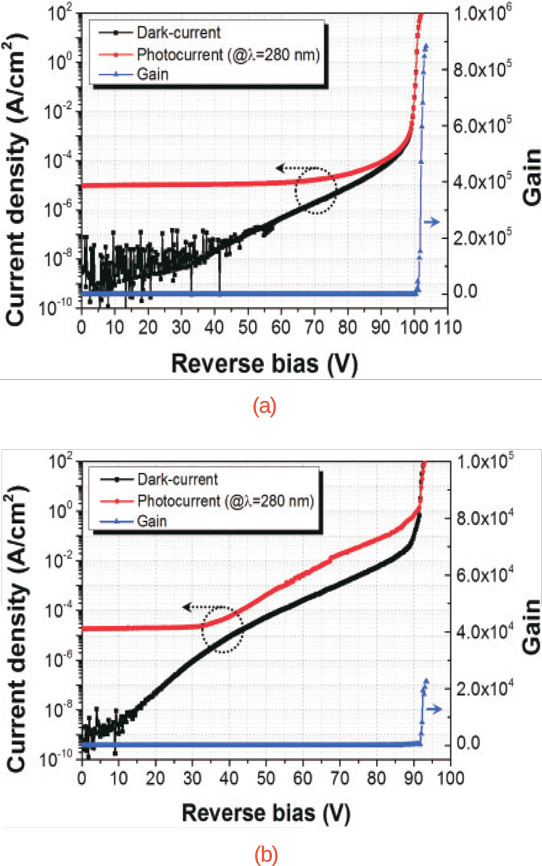
Figure 2: Reverse-bias current-voltage characteristics for 40μm-diameter (corresponding to 1256μm2) APD grown on (a) free-standing GaN substrate or (b) GaN/sapphire template.
The devices were subjected to monochromatic 280nm illumination (Figure 2). The avalanche gain was 82 with 100V breakdown and 5x10⁵ beyond 102V. For devices on GaN/sapphire, the gain was ~160 with 88V breakdown and 2x10⁴ with 93V breakdown.
The researchers comment: "Even though avalanche breakdown was observed, the avalanche gain of the UV-APD grown on the GaN/sapphire template is an order of magnitude lower than that of the UV-APD grown on the FS-GaN substrate."
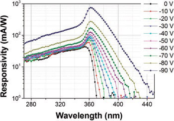 Figure 3: Reverse-bias voltage-dependent photocurrent response spectrum at room temperature for 70μm-diameter (3826μm2) APD grown on free-standing GaN substrate.
The spectral response of a 70μm-diameter APD (3847μm2) on free-standing GaN was measured under reverse bias up to 90V (Figure 3). The breakdown voltage was ~95V. The devices showed no premature micro-plasma breakdown effects in multiple current-voltage scans. By contrast, APDs on GaN/sapphire frequently showed such premature breakdown. The researchers attribute this to the higher defect density in AlGaN grown on GaN/sapphire templates.
The peak response under zero bias was 43.4mA/W at 354nm. The external quantum efficiency (EQE) was around 16%. With 80V reverse bias, the peak was 221.8mA/W at 362nm (~94% EQE).
AlGaN UV photodetectors Free-standing GaN substrate MOCVD HVPE
http://dx.doi.org/10.7567/APEX.8.122202
The author Mike Cooke is a freelance technology journalist who has worked in the semiconductor and advanced technology sectors since 1997.


