


- News
4 November 2015
Vertical conduction and ultraviolet laser diodes on bulk gallium nitride
Hamamatsu Photonics K. K. of Japan has developed 356.6nm-wavelength ultraviolet laser diodes (LDs) on bulk gallium nitride (GaN), allowing a vertical conduction scheme [Yuta Aoki, Appl. Phys. Lett., vol107, p151103, 2015]. The researchers say that there has been no previous report on aluminium gallium nitride (AlGaN) UV LDs on bulk GaN.
Instead, devices grown on sapphire have to adopt a lateral conduction scheme where the electrodes must reach the contact layers from the same side, since the substrate is electrically insulating.
The researchers comment: "The vertical conductive structure is expected to open the path to high-output-power LDs." They see potential application in broad-area striped configurations and arrayed as multiple emitters for material processing.
The vertical conduction scheme could also allow junction-down assembly for improved thermal management.
The use of bulk GaN and a vertical conduction scheme also enables cleaving of the crystal wafer to give smooth reflecting facets for the laser cavity. Sapphire substrate laser diodes are difficult to cleave and dry etching is usually adopted, which results in poor shaping of the emitted laser light.
UV LDs are of interest for chemical analysis and material processing. The alternatives such as gas or solid-state lasers suffer from problems with energy efficiency, stability, warming-up time, and compactness.
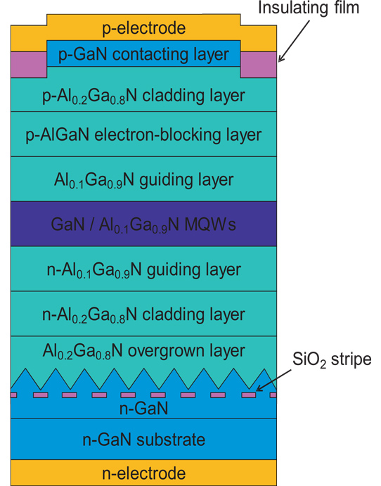
Figure 1: Schematic cross-section of GaN/AlGaN multiple quantum well (MQW) UV-LD fabricated on GaN substrate.
The epitaxial structure (Figure 1) was grown on bulk n-GaN using metal-organic chemical vapor deposition (MOCVD). Lateral overgrowth was used to improve crystal quality. This involved creating periodic silicon dioxide stripes and then growing inclined-facet GaN seed crystals in the region between the stripes. This allowed overgrowth of high-quality, crack-free Al0.2Ga0.8N, which formed the template for subsequent layers. The researchers expected the crystal quality to be similar to overgrown layers on sapphire.
The target wavelength was around 350nm, comparable to recent work on sapphire substrates.
The material was fabricated into 1.5μm ridge waveguide laser diodes. The dry etching for the ridge also exposed the p-GaN contact layer for p-electrode deposition. The n-electrode was applied after thinning of the n-GaN substrate to 100μm thickness by grinding and polishing. The mirror facets for the 300μm-long laser cavity were created by cleaving the device wafers. The facets were not coated to increase reflectivity.
The devices were tested at room temperature using 10ns pulses with 5kHz repetition. The threshold current was 250mA (56kA/cm2). A 359.6nm laser diode on sapphire has achieved 8kA/cm2 threshold. The Hamamatsu researchers believe that lower thresholds for their device on GaN could be achieved by optimizing the crystal growth and laser design.
The laser output power reached 10mW from one facet at ~300mA. The slope efficiency and external quantum efficiency (EQE) were estimated at 0.24W/A per facet and 14% for both facets, respectively.
The threshold voltage was around 20V, similar to the values obtained on sapphire. The researchers attribute the high voltage to the narrower ridge and short cavity compared with reported sapphire devices.
The spectrum of the emission peak had a full-width at half maximum (FWHM) of ~6nm below threshold (190mA) and 0.4nm above threshold (275mA). The above threshold value was close to the resolution limit of the spectrometer. The radiation was strongly transverse electric polarized, as expected from the optical gain characteristics of GaN/AlGaN MQWs and the reflectivity of the facets.
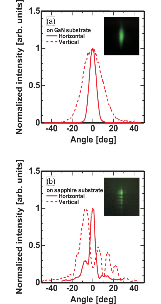
Figure 2: FFPs of UV-LD on (a) GaN substrate (with cleaved mirror facets) and (b) sapphire substrate (with etched mirror facets). Inset: photos of each FFP.
The far-field pattern (FFP) of the laser radiation was Gaussian-like in the horizontal and vertical directions, unlike devices on sapphire, which suffer from severe distortion (Figure 2). The researchers comment: "The deteriorated FFP of the UV-LD on sapphire substrate is considered to be caused by the interference between the direct beam from the mirror facet and the reflected beam from the residual terrace lying down in front of the etched mirror facet. The cleaved mirror facets provide the highly improved FFP."
Ultraviolet laser diodes Bulk GaN GaN MOCVD
http://dx.doi.org/10.1063/1.4933257
The author Mike Cooke is a freelance technology journalist who has worked in the semiconductor and advanced technology sectors since 1997.


