


- News
18 November 2015
Low-threading-dislocation AlGaN template for ultraviolet lasers
Sandia National Laboratories in the USA has reported aluminium gallium nitride (AlGaN) laser structures emitting ~350nm ultraviolet radiation from optical and electrical pumping [Mary H. Crawford et al, Appl. Phys. Express, vol8, p112702, 2015]. The researchers claim that their laser diode (LD) structure is one of only a few such reports in the sub-360nm range of wavelengths.
Pushing laser diode technology deeper into the ultraviolet would give access to applications such as fluorescence-based detection of biological agents and portable water purification.
Producing such devices is challenging since AlGaN is difficult to grow with sufficiently low threading dislocation densities (TDDs) and high enough p-type magnesium doping. Instead of using GaN templates, the Sandia team has developed low-TDD AlGaN templates on sapphire.
The researchers comment: "In contrast to GaN substrates, this approach to fabricating reduced-TDD templates can be applied to LDs across the entire AlGaN compositional range, providing a promising approach for further pushing LDs into the deep UV region."
Also, by avoiding GaN underneath the device layers, the structure is suitable for both laser diodes and bottom-emitting light-emitting diodes (LEDs). GaN absorbs radiation shorter than 365nm.
The laser material was grown by metal-organic vapor phase epitaxy (MOVPE) in a Veeco D-125 reactor. The AlGaN template was grown on c-plane sapphire (mis-cut 0.2° to m-plane), beginning with 1.9μm AlN. Next, 3μm n-Al0.32Ga0.68N was grown with a threading dislocation density of 3-4x10⁹/cm2.
Low-TDD AlGaN was produced by first etching 0.45μm-deep trenches oriented perpendicular to the major flat of the sapphire substrate to give submicron-wide mesas. The period of the trenches was 2μm. Overgrowth of 7μm n-Al0.32Ga0.68N gave a fully coalesced planar surface with 0.2nm root-mean-square roughness on a 9μm2 area. The TDD was 2-3x10⁸/cm2.
The researchers found that using standard 2-inch 0.4mm-thick sapphire substrate resulted in 70μm bowing, which in turn caused cracks to appear in the epilayers. Use of commercially available 2-inch 1.3mm-thick sapphire reduced the bowing to 15μm and eliminated cracking.
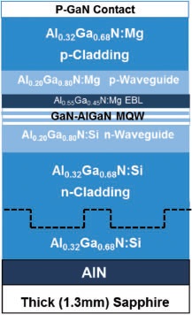 Figure 1: Schematic of laser diode heterostructure.
An optically pumped laser structure grown on the template consisted of 0.6μm cladding, 80nm waveguide, six 1.7nm GaN quantum wells separated by 7.5nm Al0.20Ga0.80N barriers, 80nm waveguide, and 10nm Al0.32Ga0.68N cap. All the layers were unintentionally doped. A 1mm-cavity laser based on this material had a threshold of 34kW/cm2 for 266nm pumping from the fourth harmonic of a pulsed Nd:YAG laser. The emission wavelength was 346nm.
For laser diodes, the researchers added an electron-blocking layer (EBL) and p-side cladding (Figure 1). Starting with the low-TDD template, the n-side of the device consisted of 230nm n-cladding and 70nm n-waveguide. The active region contained three 2.3nm GaN wells (undoped) and 7.5nm Al0.20Ga0.80N barriers (silicon-doped).
The p-side of the laser diode consisted of 12nm EBL, 60nm waveguide, 0.45μm cladding with aluminium composition graded down to a 0.32μm GaN contact.
Ridge waveguide laser diodes were fabricated with a titanium/aluminium/molybdenum/gold n-contact and palladium/gold p-contact. The facets were produced using an optimized dry/wet etch recipe. The facets were coated with high-reflectivity hafnium dioxide and silicon dioxide. The back mirror had a reflectivity of about 90% and the outcoupler reflectivity was around 80%.
Pulsed measurements were used to avoid self-heating. A device with 1mm cavity and 4μm-wide ridge emitted 352.7nm laser radiation with a threshold at 22.5kA/cm2 (Figure 2). This threshold is high compared with reports of 8kA/cm2 for 360nm wavelength, and 18kA/cm2 for 336nm.
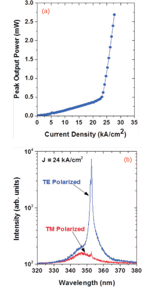
Figure 2: (a) Output power versus current density, and (b) polarization-dependent lasing spectra, for 4μm-wide ridge and 1mm-long cavity laser diode.
Simulations suggest that mode penetration into the p-GaN cap due to thin p-cladding resulted in an increased threshold.
Temperature-dependent measurements gave a characteristic temperature (T0) for the current threshold of 140K, similar to previous reports on UV lasers.
AlGaN ultraviolet lasers AlGaN UV lasers MOVPE
http://dx.doi.org/10.7567/APEX.8.112702
The author Mike Cooke is a freelance technology journalist who has worked in the semiconductor and advanced technology sectors since 1997.


