


- News
1 October 2015
Bulk gallium nitride substrate enables 4kV-breakdown vertical diode
Avogy Inc of San Jose, CA, USA has used bulk gallium nitride (GaN) substrates to create vertical p-n diodes with a breakdown voltage of more than 4kV and area-differential specific on-resistance of less than 3mΩ-cm2 [I.C. Kizilyalli et al, IEEE Electron Device Letters, published online 9 September 2015].
Bulk GaN has lower dislocation densities compared with material grown on alternative substrates such as sapphire, silicon carbide, silicon, or even free-standing GaN (where the growth substrate is removed). Controlling dislocation densities is vital to access higher breakdown voltage and lower on -resistance.
Increasing breakdown to 4kV brings potential application for ship propulsion, rail, wind, uninterruptable power supplies (UPS), geothermal instrumentation, high-voltage multipliers, military power supplies, and the power grid, according to the researchers.
Avogy has begun with p-n junction devices as a first step towards the realization of more complex vertical junction field-effect transistors (JFET) and junction barrier Schottky (JBS) diodes, which have lower turn-on voltages (<1V) and lower conduction losses.
The epitaxial structures were grown on 2-inch bulk GaN substrate with very low threading dislocation density of 104/cm2. "This is 4 orders of magnitude lower than for GaN films grown in the conventional manner on non-native substrates," according to the researchers.
The researchers designed the edge-termination, n-type drift layer and thickness to achieve junction breakdown around 5kV. In particular, the edge-termination spread the anode potential to a distance that exceeded the drift layer thickness by a factor of about 4.5. The edge-termination involved two implant steps.
The net doping density of the 40μm drift layer was 2-5x10¹⁵/cm3. "Controlling the doping of GaN to these levels by MOCVD is challenging since it is at or below the level of typical unintentional background impurities, particularly carbon," the researchers comment.
The p-region of the diode consisted of heavily magnesium-doped GaN deposited on the drift layer. The contacts were palladium/platinum.
The researchers have found that nominally c-plane oriented devices with a slight inclination towards the m-plane are optimal for reverse leakage performance and reliability. The inclination is achieved by mis-cutting by several tenths of a degree to encourage step-flow growth, avoiding the formation of screw dislocations.
Spiral growth around screw dislocations leads to unwanted large hexagonal hillocks on the GaN surface in on-axis deposition. White-light interferometry gave a mean roughness of less than 20nm over a 1mmx1mm area for an optimized substrate (B), compared with more than 50nm for a sample with lower mis-cut angle (A).
The researchers report: "The implementation of the improved substrate specification results in a marked improvement in the reverse leakage and the first demonstration of a breakdown voltage exceeding 4kV in GaN vertical p-n diodes [see Figure 1]." Last year, Avogy researchers reported devices with breakdowns up to 3.5kV and leakage about 10μA through a 0.055mm2 effective area.
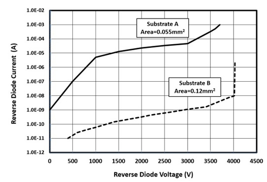
Figure 1: Reverse characteristics at 300K of GaN p-n diodes on optimized substrate B and comparison devices on unoptimized substrate A.
The team believes that further improvement of the edge-termination should lead to 5kV breakdown. The researchers calculate the field in the drift region to be 2.0-2.7MV/cm at breakdown, well short of GaN's critical field of ~5MV/cm. They conclude that the breakdown occurs in the edge-termination.
The turn-on voltage is around 3.0V, consistent with GaN's bandgap of 3.4eV. The effective device area was 250μmx500μm, as defined by the edge-termination implants. The device can handle up to 1A without substrate thinning or packaging.
In 30ms-pulsed quasi-DC operation, the area-differential specific on-resistance was 2.3mΩ-cm2 at room temperature. An increase in resistance with temperature was attributed to reduced electron mobility.
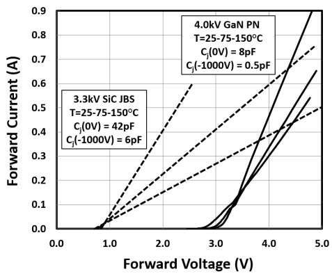
Figure 2: Forward current-voltage characteristics of 4kV GaN p-n diode and 3.3kV SiC JBS diode (dotted line) at 25-75-150°C.
The researchers compared the performance with silicon carbide junction barrier Schottky (SiC JBS) diodes (Figure 2). The junction capacitance of the GaN device was much lower, suggesting lower switching losses.
http://ieeexplore.ieee.org/xpl/articleDetails.jsp?arnumber=7247672
The author Mike Cooke is a freelance technology journalist who has worked in the semiconductor and advanced technology sectors since 1997.


