


- News
7 October 2015
Quaternary III-nitride barrier boosts two-dimensional electron gas
Researchers based in France claim the best two-dimensional electron gas (2DEG) properties ever reported for III–nitride (III-N) semiconductor structures [Farid Medjdoub etal, Appl. Phys. Express, vol8, p101001, 2015].
The team from Institute of Electronic, Microelectronic and Nanotechnology (IEMN) and Thales Research and Technology sees potential telecommunication, healthcare, space and military 30GHz+ applications based on higher power densities, increased efficiency over a range of frequencies, high performance over wide bandwidths, and higher thermal conductivity.
Such 2DEGs are used as conduction channels in high-electron-mobility transistors (HEMTs) and other devices. The 2DEG forms near the interface between gallium nitride (GaN) and a barrier structure. Normally the barrier consists of a wider-bandgap material such as aluminium gallium nitride (AlGaN) – a ternary III-nitride material.
IEMN has previously developed indium aluminium nitride (InAlN) as an alternative that can be lattice matched with GaN. However, this ternary material is difficult to grow with sufficient uniformity. Problems arising from non-uniformity include alloy scattering, interface roughness, and carrier interactions with optical and acoustic phonons.
The IEMN/Thales team has combined the advantages of AlGaN and InAlN by using a quarternary InAlGaN barrier, allowing for lattice matching.
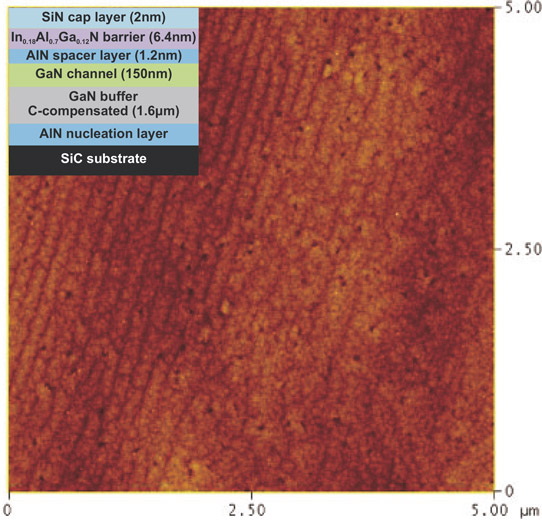
Figure 1: 5μmx5μm AFM image of SixNy/InAlGaN/AlN/GaN HEMT heterostructure. Inset shows cross section of fabricated device.
The InAlGaN/AlN/GaN structure (Figure 1) for creating a 2DEG was grown using low-pressure metal-organic chemical vapor deposition (LP-MOCVD) on 4-inch semi-insulating silicon carbide (SiC). The InAlGaN had 18% In content and 12% Ga content, giving material lattice matched to GaN. The silicon nitride (SiN) cap was produced in-situ, using ammonia and silane precursors.
The researchers describe the resulting material surface as 'mirror-like' with roughness of 0.27nm root-mean-square, according to atomic force microscopy (AFM). A low defect density and atomic steps were found.
Table 1: Characteristics of 2DEG at 1.9x10¹³/cm2 sheet carrier density.
| Room temperature | 77K | |
| Mobility | 1800cm2/V-s | 6800cm2/V-s |
| Sheet resistance | 191Ω/square | <50Ω/square |
Mobility, carrier density and sheet resistance were assessed using Hall measurements on van der Pauw structures and mercury-probe capacitance–voltage measurements at room temperature and 77K (Table 1). Benchmarked against the work of others (Figure 2), the team describes its work as 'state-of-the-art'.
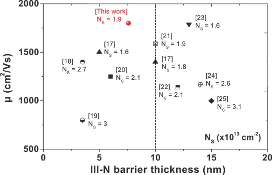
Figure 2: Benchmark of RT electron mobility as a function of barrier thickness (including spacer interlayer) in III–N-based HEMT structures. The carrier density Ns is indicated for each reference.
The researchers comment further: "A real breakthrough in terms of electrical and structural properties of the SiN/InAlGaN/AlN/GaN heterojunction has been obtained, as compared with the InAlN/AlN/GaN heterojunction (typical values of μ300K are about 1300cm2V−1 s−1 for 1.3x1013cm−2)."
The team looks forward to optimizations of the thickness and growth conditions of the AlN spacer as a means to achieving higher mobility. The SiN layer is seen as contributing to the high 2DEG performance through preventing strain relaxation and early passivation of surface charges.
The researchers add: "The electron mobility improvement in this ultrathin barrier heterostructure is attributed to the optimization of the material quality showing low interface roughness owing to the introduction of Ga into the barrier layer, the use of an in-situ-grown SixNy cap layer, and the introduction of an optimized AlN spacer layer."
HEMT devices were fabricated with annealed titanium/aluminium/nickel/gold ohmic contacts on the InAlGaN barrier layer and 250nm nickel/gold Schottky gate. Isolation was achieved using nitrogen implantation. The gate–source and gate–drain spacings were 0.3μm and 2μm, respectively. The device width was 50μm.
The maximum DC drain current density was 1.5A/mm at +2V gate potential. The peak transconductance was more than 300mS/mm.
The off-state leakage for –5V gate was well below 1μA/mm. The off-state broke down at about 50V drain bias.
Frequency measurements gave current-gain and power-gain extrinsic cut-off frequencies (fT/fmax) of 60GHz and 190GHz, respectively.
The researchers comment: "A further reduction in contact resistances should result in an increase in extrinsic transconductance and, thus, a significant improvement of frequency performance."
http://dx.doi.org/10.7567/APEX.8.101001
The author Mike Cooke is a freelance technology journalist who has worked in the semiconductor and advanced technology sectors since 1997.


