


- News
1 October 2015
Polarized white light-emitting diode without phosphor conversion
University of California, Santa Barbara (UCSB) researchers have developed polarized white light-emitting diodes (LEDs) that do not use phosphors [S. J. Kowsz et al, Appl. Phys. Lett., vol107, p101104, 2015].
Such devices could lead to less power consumption in liquid-crystal displays (LCDs), which depend on polarized light for their operation. Presently, unpolarized light from white LED back-lighting is put through a polarizing sheet to give the polarized light for phase shifting by the liquid crystal. The polarization cuts the light power by at least half. Even if the light was only partially polarized, the loss from transmission through a polarizer could be reduced.
White LEDs are commercially produced using c-plane (0001) III-nitride epitaxial growth, giving unpolarized devices. Growth of the crystal structure in other orientations gives light emission that is partially polarized.
Although indium gallium nitride (InGaN) should theoretically give light emission across the visible spectrum, present commercial technology is limited to wavelengths shorter than green (495-570nm). White LEDs generally use a narrow blue emission in combination with phosphors that convert some of the blue photons (e.g. 435-455nm) into a broad range centered on yellow wavelengths (e.g. 500-650nm).
Instead of phosphors, the UCSB device uses a multiple quantum well (MQW) to convert some blue photons into longer wavelengths by photoluminescence/optical pumping. Such structures have been explored by a number of research groups using c-plane III-nitrides, but these naturally lead to unpolarized light.
The UCSB metal-organic chemical vapor deposition (MOCVD) epitaxial structure (Figure 1) was grown on semi-polar (20-2-1)/(20-21) free-standing GaN from Mitsubishi Chemical Corp. The 7.5mmx7.5mm substrate was polished on each side. The 12nm single quantum well InGaN LED was grown first on the (20-2-1) side. The conversion structure with three quantum wells was grown on the (20-21) side.
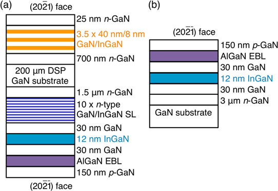
Figure 1: Schematic cross-section of epitaxial structure of (a) double-sided, electrically injected and optically pumped semi-polar device and (b) standard electrically injected semi-polar blue LED.
The MQW structure on the (20-21) side was grown at low temperature to enable high indium content incorporation. The final GaN cap layers were grown at the same temperature to avoid decomposition of the underlying InGaN. If such MQWs were grown in an LED structure, the final p-contact layers would need to be grown at higher temperature to give sufficient p-type conductivity to inject holes, resulting in quality degradation of the InGaN wells.
The contact for the p-GaN consisted of palladium/silver/nickel/gold. The n-contact was a soldered indium dot. The n-type GaN/InGaN superlattice (SL) was designed to assist lateral conduction from the n-contact.
The device produced a narrow peak from the LED section with peak wavelength at 440nm (Figure 2). The conversion section produced a broader spectrum with a maximum at 560nm. The conversion peak is narrower than usually produced with phosphor conversion, but the researchers believe that the MQW structure could include wells with longer wavelength emission to achieve a comparable spectrum.
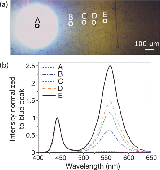
Figure 2: (a) Optical micrograph of electrically injected device based on epitaxial structure in Figure 1 (a), indicating measurement locations. (b) Electroluminescence spectra at different locations normalized to corresponding blue emission peak.
The color balance across the device was not uniform with emission near the contact (A) being more blue than that further away. The 1931 Commission Internationale de l'Eclairage (CIE) x, y chromaticity co-ordinates were, in order A-E, (0.16, 0.03), (0.24, 0.21), (0.28, 0.29), (0.30, 0.33), and (0.33, 0.39). The C position gave emission close to Planck black-body color content for 9859K.
The researchers report: "Ongoing work is focused on increasing the intensity of the long-wavelength emission from the optically pumped QWs relative to the blue emission from the LED in order to achieve uniform white light emission. The color uniformity can be improved by increasing the yellow light emission from the optically pumped QWs and/or reducing the amount of blue light that is extracted."
For light collected at point C, the researchers found a polarization ratio of 0.4, comparing light polarized along [1-210] and [-101-4]. Spectral analysis found that the polarization ratio of the blue radiation was 0.6. The ratio for the optically pumped layers was 0.33.
Previous research has found higher optical polarization in devices grown on (20-2-1) substrates, compared with (20-21). The (20-2-1) polarization also increases with indium content, while the polarization of (20-21) wells remains relatively constant. The reason for such behavior is unknown.
Improving the extraction efficiency may not be straightforward, since the common technique of surface roughening would tend to reduce polarization. The researchers suggest that photonic crystals could be a way to tackle this problem.
LCDs LEDs LED back lighting GaN InGaN
http://dx.doi.org/10.1063/1.4930304
The author Mike Cooke is a freelance technology journalist who has worked in the semiconductor and advanced technology sectors since 1997.


