


- News
15 September 2015
Improving performance of magnesium doping for p-type gallium nitride
Taiwan's National Tsing Hua University has been studying ways to improve the performance of p-type gallium nitride (p-GaN) in terms of hole density and contact resistance with nickel/gold [Bo-Sheng Zheng et al, J. Appl. Phys., vol118, p085706, 2015].
Low hole density is a particular problem with p-GaN due to the high activation energy of magnesium acceptors. A further problem is parasitic incorporation of hydrogen that further kills hole densities.
Annealing is often used to drive out hydrogen and improve performance. High temperatures can damage the device structure, particularly the indium gallium nitride (InGaN) layers used in light-emitting diodes.
The researchers assessed the relative merits of rapid thermal and laser annealing, along with the use of a nickel cap to enhance desorption of hydrogen. Nickel caps could also improve the surface integrity in laser annealing, where scanning normally produces surface damage.
GaN was grown on 2-inch c-sapphire with a p-i-n structure (Figure 1) by metal-organic chemical vapor deposition (MOCVD). The hole density in the magnesium-doped region, according to Hall measurements, was 1.8x10¹⁷/cm3. The electron density in undoped GaN was in the range 1-3x10¹⁶/cm3.
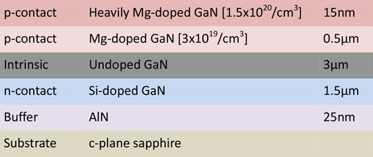
Figure 1: Epitaxial structure.
Four magnesium-doping activation schemes were studied involving different combinations of rapid thermal annealing (RTA) or neodymium-doped yttrium aluminium garnet (Nd:YAG) laser annealing, with or without nickel cap (Table 1). The samples were cleaned before application of the nickel caps. After annealing, the nickel caps were removed with aqua regia or hydrochloric acid.
Table 1: Electrical characteristics of samples subjected to different heat treatments.
| RTA | Laser (50kHz, 600mJ/cm2) | Hole density | Specific contact resistance | Remarks | |
| As-grown | n/a | n/a | 1.8x10¹⁷/cm3 | ~1x10⁻²Ω-cm2 | n/a |
| Sample A | Without Ni 900°C, 2 min. | n/a | 5.1x10¹⁷/cm3 | 2.8x10⁻³Ω-cm2 | n/a |
| Sample B | n/a | Without Ni | 3.2x10¹⁷/cm3 | 2.3x10⁻³Ω-cm2 | Surface deformation |
| Sample C | Ni cap (50nm) 500°C, 10 min. | n/a | 4.4x10¹⁷/cm3 (Ni/Au contacts) | 3.5x10⁻²Ω-cm2 | Formation of Ga-O-Ni compound |
| Sample D | n/a | Ni cap (200nm) | 3.8x10¹⁷/cm3 | 1.6x10⁻⁴Ω-cm2 | n/a |
For testing, annealed nickel/gold ohmic contact metals were applied. Diodes were fabricated with mesa etching. The Hall measurements for the hole density were carried out in the van der Pauw configuration with indium ball electrodes. The specific contact resistance was measured by the circular transmission-line method.
All the annealing processes increase hole density by a factor of 2-3x. The RTA process gives higher hole density than the laser activation. The researchers write: "We attribute the increase in hole density to a better activation of Mg, most likely due to the break-off of hydrogen from Mg at high annealing temperatures. The parasitic hydrogen attached to Mg is incorporated during the epitaxial crystal growth of GaN."
The contact resistance of the RTA sample C with nickel cap was worse than the as-grown sample. The other treated samples performed better, but there was not a straightforward inverse relation between hole density and contact resistance. The team comments: "This seemingly puzzling contradiction in numbers suggests that the hole concentration depth profiles in heat treated samples may not be uniform. Instead, there might be a gradient in the profiles tapering from the surface toward bulk. It is possible that a steeper gradient may yield a higher surface concentration but actually a smaller overall sheet carrier density."
The problem with the sample C contact resistance was attributed to a gallium-oxygen-nickel compound, which is thought to interrupt carrier transport. By contrast, laser annealing with nickel cap (sample D) was found to be free of such parasitic compounds, according to transmission electron microscopy (TEM) that shows a smooth rather than rough surface.
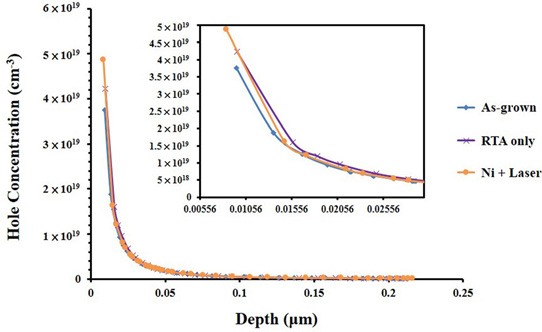
Figure 2: Profiles of hole concentration versus depth for p-GaN subject to RTA without nickel caps and laser annealing with nickel caps.
The hole density relation with depth was probed with capacitance-voltage measurements (Figure 2). The results showed enhanced density near the surface.
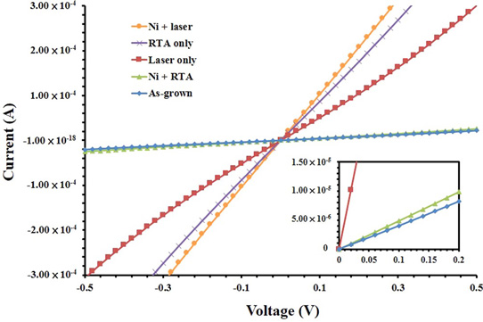
Figure 3: Forward current-voltage characteristics at room temperature of p-i-n diodes.
Current-voltage curves for nickel/gold contacts on p-GaN and for the p-i-n mesa diodes (Figure 3) showed improved current flow for annealed samples. The pin A diode with highest current was for laser annealing with nickel cap. The B diode was for RTA annealing, and C for as-grown. The voltage drop for 100A/cm2 current was 3.70V, 3.94V and more than 4.0V for diodes A-C in order. The ideality factors were between 2.6 and 2.8. The breakdown of all devices occurred around 600V.
http://dx.doi.org/10.1063/1.4929522
The author Mike Cooke is a freelance technology journalist who has worked in the semiconductor and advanced technology sectors since 1997.


