


- News
13 April 2016
Gallium arsenide on V-groove silicon template for photonics and electronics
Researchers in Hong Kong and USA have developed indium arsenide (InAs) quantum dot (QD) microdisk lasers directly integrated on silicon (Si) with performance comparable to the best reported for similar devices on gallium arsenide (GaAs) substrates [Yating Wan et al, Optics Letters, vol41, p1664, 2016]. The team from Hong Kong University of Science and Technology (HKUST), University of California Santa Barbara (UCSB) and Harvard University claims the devices as the first 1.3μm room-temperature continuous-wave InAs QD microdisk lasers epitaxially grown on industry-compatible Si (001) substrates without offcut.
The researchers believe that such direct integration on silicon could pave the way to low-cost and compact photonic integrated circuits (PICs) on mainstream silicon platforms such as silicon-on-insulator.
The teams first created GaAs on V-grooved Si (GoVS) templates. By growing GaAs first as nanowires in the grooves, followed by coalescence, the resulting template was of high quality and free of anti-phase domains. The technique avoids the usual offcut method for reducing anti-phase domains. Offcutting compromises compatibility with CMOS manufacturing.
The 1μm GaAs template layer was grown using metal-organic chemical vapor deposition (MOCVD) on exactly oriented (001) Si. The lattice mismatch between the GaAs and Si groove wall was 4.1%. The technique also avoids the use of thick buffer layers and dislocation filters, which are optically absorbing.
The transition between the structures was accommodated with a few nanometers of stacking faults (SFs). The SFs were trapped in this region by 'diamond-shaped-pockets' near the top of the grooves.
The researchers see analogies with the aspect ratio trapping (ART) used to integrate III-V high-mobility channel fin field-effect transistors on silicon: "The GoVS templates can thus be envisaged as an extension of III–V fin arrays for optoelectronic devices requiring large active regions, suggesting the possibility of co-integration of silicon photonic and electronic circuits onto the same chip. More importantly, the highly scalable growth technique presented here is extendable to the [indium phospide] InP material system, and can be potentially used for the growth of various heterostructures with ternary and quaternary materials, quantum wells, or quantum dots on silicon, as evidenced by a recent report of InP distributed feedback laser arrays directly grown on silicon."
Since the surface of the GoVS template had low roughness of ~2nm root-mean-square over 5μmx5μm atomic force microscope (AFM) scans, there was no need for chemical mechanical polishing (CMP). The researchers estimate the GaAs defect density at ~108/cm2, commenting: "Both TEM and x-ray diffraction suggest a three- to four-fold reduction of defects, as compared to blanket heteroepitaxy of GaAs on offcut Si wafers."
The microdisk laser structure (Figure 1) was grown by molecular beam epitaxy (MBE). The optically active InAs quantum dots (QDs) were created in five In0.15Ga0.85As well layers separated by 37.5nm GaAs barriers. The dot-in-well (DWELL) layers had a dot density of 4.3x10¹⁰/cm2.
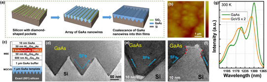
Figure 1: (a) Procedure for growing antiphase-domain-free GaAs thin films. (b) AFM image of coalesced GaAs thin film grown on nanowire array. Vertical bar is 25nm. (c) Schematic of as-grown structure of microdisk lasers. (d)–(f) Cross-sectional transmission electron microscope (TEM) images of V-groove. (g) Room-temperature photoluminescence spectra of as-grown structures on GoVS template and GaAs substrate.
Optical pumping of the epitaxial structure at 4.7kW/cm2 resulted in peak photoluminescence around 2.5x lower than QDs grown on GaAs substrate. The peak of the spectrum was also blue-shifted by about 18nm in wavelength. The researchers comment: "The high pump power results in the saturation of ground-state emission which centers in the 1.3μm telecommunication band and gives rise to emissions from excited states on the high-energy side."
Microdisks were created by using 4μm silica beads dispersed on the epitaxial material as hard masks for ion-assisted etching to give cylinder mesas. The silicon dioxide of the beads was removed in an ultrasonic bath of acetone. Further etching with hydrofluoric acid solution created a pedestal structure by selectively etching the high-aluminium Al0.7Ga0.3As layer. The undercut distance was about 1.6μm. The pedestal was designed to confine the optical modes to the disk and avoid evanescent coupling of electromagnetic energy into the underlying substrate.
The microdisk lasers were characterized with pumping at 532nm wavelength by a diode laser under continuous wave operation. The diode laser spot was focused into a 4μm diameter. The threshold power for lasing was estimated at ~200μW (Figure 2). Microdisk lasers were also produced on GaAs substrate.
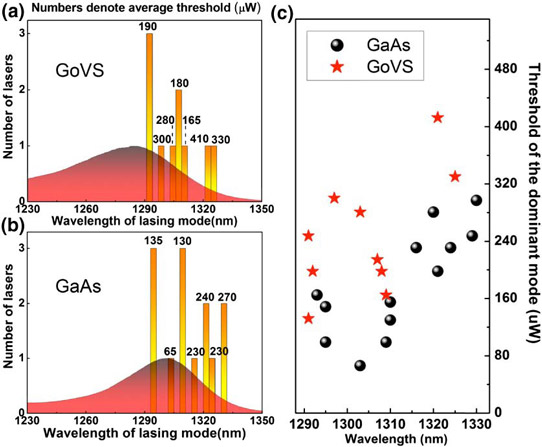
Figure 2: (a), (b) Histograms of lasing wavelength for each measured device on GoVS and GaAs, respectively. Average lasing threshold of devices within each histogram bar is denoted by top number. Normalized photoluminescence spectrum of unprocessed samples in red. (c) Microdisk lasing threshold plotted as function of wavelength.
The researchers comment: "The spread of the central wavelengths in the measured samples is foreseeable, if one considers the distribution of QD density and their varied overlap with the modes of the microdisks. The threshold is lowest around 1.3μm, where lasing takes place at a wavelength close to the center of the broad gain spectrum, providing the strongest spatial overlapping of emitters to the surrounding cavity."
The spread in threshold was from 130μW up to 410μW with 250μW average (50μW per QD layer). The average for microdisks on GaAs substrate was about 1.4x lower at 180μW. The researchers see their GoVS devices as being comparable in performance with the best reported values for InAs QD microdisk lasers with the same cavity size on GaAs.
The team believes better performance could come from enhancing the quality of the coalesced GaAs films and improving the uniformity of the quantum dots.
InAs quantum dot microdisk lasers InAs GaAs substrates
http://dx.doi.org/10.1364/OL.41.001664
The author Mike Cooke is a freelance technology journalist who has worked in the semiconductor and advanced technology sectors since 1997.


