- News
6 April 2016
Vertical gallium nitride Schottky diode combining high current/breakdown
HRL Laboratories LLC in the USA has developed a gallium nitride (GaN) vertical tunneling Schottky barrier diode (TBS) that gives good combined on and off performance, compared with vertical Schottky barrier diodes (SBDs) [Y. Cao et al, Appl. Phys. Lett., vol108, p112101, 2016].
Gallium vertical SBDs suffer from trade-offs between on-current and reverse bias breakdown. By applying a thin layer of aluminium gallium nitride (AlGaN) as a tunneling barrier, the HRL team allowed a more highly doped drift layer to be used, increasing on-current, without compromising the breakdown voltage.
Vertical Schottky diodes and other power devices built using GaN technology could lead to higher current density handling and smaller components compared with the lateral structures that have been the focus of most development until recently.
The new interest in vertical structures has been enabled by reductions in defect densities due to the commercial availability of free-standing and bulk GaN substrates. However, the initial work has largely been on p-n junction diodes that have high turn-on voltages of ~3V arising from the wide bandgap (~3.4eV). High turn-on voltage devices suffer from large conduction losses.
Schottky barrier diode structures can reduce turn-on to less than 1V, but usually with lower breakdown voltages. SBDs also have faster performance.
The wide bandgap and high electron mobility of GaN compared with silicon are attractive for reduced size and weight power devices operating at higher frequency.

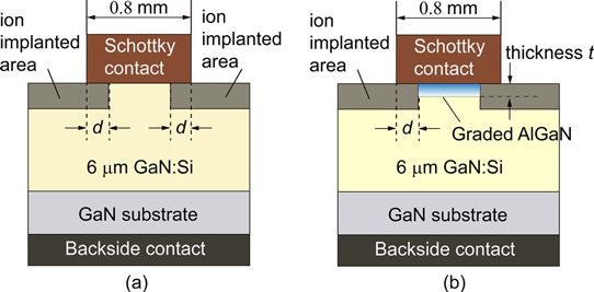
Figure 1: Schematic structures for (a) control sample A, and sample B with high doping, and (b) the sample C with graded AlGaN cap layer.
The drift layer of the HRL devices (Figure 1) was 6μm silicon-doped GaN, grown by metal-organic chemical vapor deposition (MOCVD) at 1040°C. The substrate was 2-inch c-plane free-standing bulk n-GaN. The carbon concentration was reduced to less than 3x10¹⁵/cm3 by using a growth pressure of 300Torr and a V/III precursor ratio of 4777.
The tunnel barrier consisted of 5nm graded AlGaN layer with Al-concentration varying from 0% to 23%. This was achieved by linearly ramping the flow of trimethyl-aluminium precursor.
Edge-termination of the SBDs was achieved with ion implantation. The edge-termination region overlapped 10μm with the 0.8mmx0.8mm nickel/gold Schottky contact. A non-alloyed ohmic contact was applied to the back-side of the wafer.
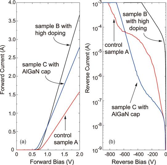
Two SBDs were produced with different silicon-doping levels of the drift layer (A and B): ~1x10¹⁶/cm3 and ~3x10¹⁶/cm3, respectively. The tunneling SBD (TBS), sample C, had the same silicon doping as sample B.

Figure 2: Plots of forward current (a) and reverse current (b) as function of bias.
The TBS allowed a higher on-current compared with sample A, while maintaining good breakdown performance under reverse bias (Figure 2, Table 1).
Table 1: Performance metrics for HRL vertical Schottky diodes
| Sample | A | B | C (TBS) |
| Free electron density | ~7.5x10¹⁴/cm3 | 2.6x10¹⁵/cm3 | 2.9x10¹⁵/cm3 |
| Current (Ion) at 1.6V forward voltage (Vf) | 1.07A | 2.51A | 1.95A |
| Reverse bias breakdown at 1mA | >800V | ~345V | 700V |
| Turn-on voltage | 0.77V | 0.75V | 0.67V |
| Total specific on-resistance | 4.94mΩ-cm2 | 2.17mΩ-cm2 | 3.06mΩ-cm2 |
The HRL researchers compare their TBS device with the performance of Cree's commercial silicon carbide (SiC) junction barrier Schottky diode (JBS, Table 2): "It can be seen that, with a slightly smaller area, our TBS diode could achieve twice the on current of the JBS diode at Vf = 1.6V, or reach the same on-current of 1A at a 28% lower forward bias. This result indicates that it is possible for a GaN-based Schottky diode to further reduce the conduction loss and improve the efficiency in current 600V systems, where SiC-based diodes are used."
Table 2: Comparison of key parameters between HRL's tunneling barrier Schottky diode and Cree's 600V JBS.
| Die area (mm2) | Ion (A) @ Vf = 1.6V | Vf (V) @ Ion = 1.0A | |
| HRL GaN TBS | 0.64 | 2.0 | 1.15 |
| Cree SiC JBS (CPWR-0600S001) | 0.71 | 1.0 | 1.6 |
SiC has similar material properties to GaN of wide bandgap and high electron mobility.
GaN vertical tunneling Schottky barrier diode GaN AlGaN HRL Laboratories GaN substrates
http://dx.doi.org/10.1063/1.4943946
The author Mike Cooke is a freelance technology journalist who has worked in the semiconductor and advanced technology sectors since 1997.


