- News
8 April 2016
III-nitride high-electron-mobility transistors on flexible tape
Researchers in France claim the first demonstration of 10GHz large-signal microwave power performance for flexible aluminium gallium nitride (AlGaN) barrier high-electron-mobility transistors (HEMTs) [S. Mhedhbi et al, IEEE Electron Device Letters, published online 16 March 2016]. The devices were produced on low-cost silicon substrates and transferred to flexible tape.
The team comments that their work "demonstrates the capability of flexible GaN-based HEMTs for the development of applications requiring mechanical flexibility, high-frequency operation as well as high-power performance."
The researchers are at Institut d'Electronique de Microélectronique et de Nanotechnologie (IEMN), Centre de Recherche sur l'Hétéro-Epitaxie et ses Applications, and 3M France Company.
The material for the HEMTs was grown by molecular beam epitaxy (MBE) on high-resistivity (111) silicon: 44nm AlN nucleation, 250nm Al0.15Ga0.85N and 130nm AlN stress mitigation, 1.73μm GaN buffer, 1nm AlN spacer, 10nm Al0.29Ga0.71N barrier, and 0.5nm GaN cap.
The ohmic source-drain electrodes consisted of annealed titanium/aluminium/nickel/gold. Devices were isolated with nitrogen ion implants.
The 100nm-long nickel/gold gate was T-shaped. The gate width was 2x50μm (100μm total). The gate-source and source-drain spacings were 1μm and 2.75μm, respectively.
The HEMTs were passivated with plasma-enhanced chemical vapor deposition (PECVD) of silicon nitride and silicon dioxide dielectrics. The contact pads were titanium/gold.

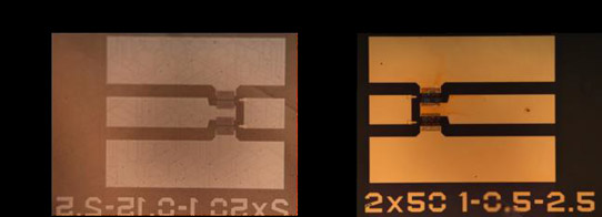
Figure 1: Optical images of device (a) backside after silicon etching and (b) after transfer onto 3M flexible tape.
The silicon substrate was removed by bonding the front-side of the wafer to a sapphire carrier with photoresist. Chemical-mechanical lapping ground down 100μm of the silicon wafer. Dry etching removed the remaining silicon down to the AlN nucleation layer that was used as etch stop (Figure 1).
The thinned devices were transferred to thermally conductive tape under development by 3M. The tape is designed to withstand temperatures up to 260°C for short periods (of the order of minutes). The tape was 250μm thick.
The elastomeric-silicone carrier material of the tape was highly loaded with thermally conductive filler. One side of the tape was coated with high-temperature-resistance silicone adhesive. The tape was also designed to be chemically resistive to common solvents.
The sapphire carrier was removed by dissolving the photoresist adhesion layer in acetone.
Hall measurements of transferred material gave a sheet resistance of 437Ω/square, a high mobility of 1831cm2/V-s, and sheet carrier density of 9x10¹²/cm2.
Coplanar propagation waveguides (CPWs) were also fabricated on the tape with gold/titanium metal. A 1mm-long CPW had as low as 0.2dB/mm loss at 10GHz. This value is comparable to the values for microwave circuits on high-resistivity silicon.
The maximum drain current for the HEMTs was 620mA/mm at 3V drain bias and 0V gate potential. At the same drain bias, the maximum extrinsic transconductance was 293mS/mm at -2.2V gate potential. The pinch-off voltage was estimated at -3.3V. The researchers comment: "Despite the lack of materials and technology developments for transferred devices, the drain current ratio ION/IOFF ratio is equal to 105."

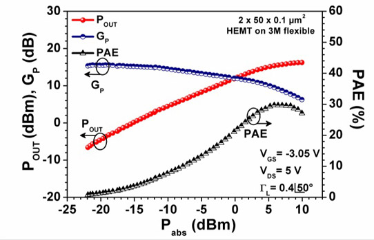
Figure 2: Output power, power gain and power-added efficiency versus absorbed power at 10GHz for a 2x50μmx0.1μm AlGaN/GaN HEMT on 3M flexible tape at 5V drain.
Using the maximum transconductance parameters as bias point (3V drain, -2.2V gate), the cut-offs for current gain (FT) and Mason's gain (FMAX, extrapolated from 67GHz maximum RF measurement with assumed -20dB/decade fall off) were 38GHz and 75GHz, respectively.
Large-signal measurements were made with 10GHz continuous wave (CW) operation of an active load-pull setup. The drain and gate bias points were 5V and -3V, respectively, giving AB-class amplification. The linear power gain was 15.8dB. The saturated output power and power-added efficiency were 0.42W/mm and 29.6%, respectively.
"To our knowledge, this performance constitutes the current state of the art at 10 GHz for flexible devices," the team writes. The researchers believe that the saturated power density figure represents the first such result ever reported in the field of flexible electronics. The team also suggests that improved performance and reliability could come from tape with better thermal conductivity.
AlGaN HEMTs AlGaN HEMTS MBE PECVD
http://ieeexplore.ieee.org/xpl/articleDetails.jsp?arnumber=7434553
The author Mike Cooke is a freelance technology journalist who has worked in the semiconductor and advanced technology sectors since 1997.


