


- News
22 April 2016
Accuracy of LayTec EpiTT Gen3's XRD-referenced nk database improved for InP-based materials
Together with Dr Tony SpringThorpe's team at the National Research Council of Canada and Christoph Hums and his co-workers at Fraunhofer HHI (Heinrich Hertz Institute) in Berlin (a research center for communication systems, digital media and services), in-situ metrology system maker LayTec AG of Berlin, Germany has further improved the accuracy level of its nk database for the two quaternary material systems InGaAsP (indium gallium arsenide phosphide) and InGaAlAs (indium gallium aluminium arsenide).
Indium phosphide (InP)-based materials exhibit higher electron mobility and higher frequency response compared to gallium arsenide (GaAs). This makes the InP heterojunction bipolar transistor (HBT) a good candidate for next-generation transimpedance amplifiers in optical fiber communications and for 5G applications. Moreover, since an InP HBT's base bandgap energy is much lower than that of a GaAs HBT's, the InP-based device's turn-on voltage and related power consumption are significantly lower.
However, high-yield metal-organic chemical vapor deposition (MOCVD) growth of device-grade quaternary InGaAsP and InGaAlAs structures precisely lattice matched to InP is rather challenging, especially on larger wafers. The solution is in-situ process control based on accurate high-temperature quaternary nk data, says LayTec.
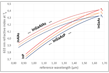
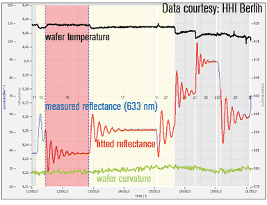
Fig. 1: Control of device-related InGaAsP and InGaAlAs film growth on InP. When lattice-matched growth is validated by in-situ wafer bow sensing, both quaternary material systems can be treated as an effective quasi-ternary mixture: (InGaAs)x(InP)1-x and (InGaAs)x(AlGaAs)1-x, respectively. (a) The respective composition range (x=0…1) covers the reference (PL) wavelength range 0.92–1.65µm for InGaAsP and 0.85–1.65µm for InGaAlAs. The three lines for each material system give the 633nm refractive index at three wafer temperatures. (b) The quaternary/ternary layers (steps 17–29) are lattice matched to InP (step 15), as can be seen from the unchanged wafer curvature (green line). Hence, the measured 633nm reflectance data (blue line) of an InP/InGaAsP device structure can be exactly fitted (red line), yielding all compositions x and all growth rates. The –3K reduction in wafer temperature due to the changed As/P ratio is a real effect.
Figure 1 gives selected examples. Figure 1a shows the 633nm refractive index of InGaAsP and InGaAlAs in the full composition range at three relevant growth temperatures, T1<T2<T3. With n(x,T) and k(x,T) available for the full range of lattice-matched quaternary compositions, precise and quantitative process control becomes straightforward, says LayTec. Figure 1b demonstrates the smooth fit to in-situ reflectance of a device structure. In-situ sensing of wafer bow (the green line in Figure 1b) using LayTec's EpiCurveTT system validates the lattice-matched growth.
For this highly precise nk database, growth rates and accurate lattice match were carefully matched to ex-situ x-ray diffraction (XRD). Wafer temperatures were measured using the EpiTT system, which had been previously calibrated using LayTec's AbsoluT temperature calibration tool.
LayTec Metrology MOCVD EpiCurveTT EpiTT HHI


