


- News
25 April 2016
NREL theory overcomes barrier to using 2D semiconductors in electronic and optoelectronic devices
The US Department of Energy's National Renewable Energy Laboratory (NREL) says that it has uncovered a way to overcome a principal obstacle in using two-dimensional (2D) semiconductors in electronic and optoelectronic devices (Yuanyue Liu, Paul Stradins and Su-Huai Wei, 'Van der Waals metal-semiconductor junction: weak Fermi level pinning enables effective tuning of Schottky barrier', Science Advances, vol.2, no.4, e1600069).
2D semiconductors such as molybdenum disulfide are only a few layers thick and are considered promising candidates for next-generation devices. Researchers must first overcome limitations imposed by a large and tunable Schottky barrier between the semiconductor and a metal contact. The barrier, at the metal/semiconductor junction, creates an obstacle for the flow of electrons or holes through the semiconductor.
The NREL team discovered that the height of the Schottky barrier can be adjusted - or even made to vanish - by using certain 2D metals as electrodes. Such adjustments are not possible with conventional three-dimensional metals because of a strong Fermi-level pinning (FLP) effect occurring at the junction of the metal and the semiconductor, due to electronic states in the semiconductor bandgap that are induced by the metal. Increasing the flow of electrons or holes through a semiconductor reduces power losses and improves the device performance.
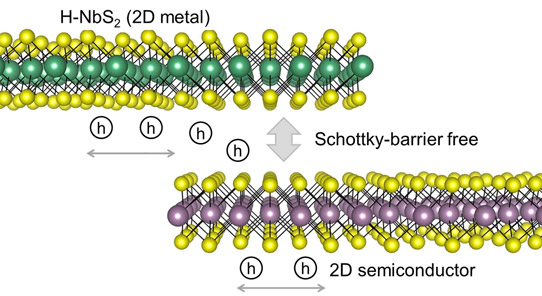
Picture: 2D H-NbS2 can form a Schottky-barrier-free contact with 2D semiconductor for hole transport.
The NREL theorists considered a family of 2D metals that could bind with the 2D semiconductors through van der Waals (vdW) interaction. Because this interaction is relatively weak, the metal-induced gap states are suppressed and the FLP effect is negligible, so the Schottky barrier becomes highly tunable. By selecting an appropriate 2D metal/2D semiconductor pair (such as H-NbS2/WSe2 for hole conduction), one can reduce the barrier to almost zero.
The researchers noted that using a 2D metal as an electrode would also prove useful for integrating into transparent and flexible electronics because the 2D metal is also transparent and flexible. They also noted that the junction of 2D metal and 2D semiconductor is atomically flat and can have fewer defects, which would reduce carrier scattering and recombination.
The NREL research predicts that the hexagonal phase of niobium disulfide (NbS2) is the most promising for hole injection into a 2D semiconductor, and heavily nitrogen-doped graphene can enable efficient electron injection.
The research was funded by the Department of Energy's Office of Energy Efficiency and Renewable Energy. The work used computational resources at NREL and the National Energy Research Scientific Computing Center.
http://advances.sciencemag.org/content/2/4/e1600069


