- News
21 April 2016
UCSB-led team reports first quantum cascade laser on silicon
A team led by Alexander Spott of University of California, Santa Barbara – in collaboration with the US Naval Research Laboratory (NRL) and the University of Wisconsin, Madison – has fabricated what is said to be the first quantum cascade laser (QCL) on silicon. The advance may have applications that span from chemical bond spectroscopy and gas sensing to astronomy and free-space communications.
Integrating lasers directly on silicon chips is challenging, but it is much more efficient and compact than coupling external laser light to the chips. The indirect bandgap of silicon makes it difficult to fabricate a laser from silicon, compared with diode lasers fabricated from III-V materials such as indium phosphide (InP) or gallium arsenide (GaAs). By directly bonding a III-V layer on top of the silicon wafer and then using the III-V layers to generate gain for the laser, this same research group previously integrated a multiple quantum well (MQW) laser on silicon that operates at 2µm. However, limitations in diode lasers prevent going to longer wavelengths where there are many more applications, so the group instead turned its attention to using quantum cascade lasers.
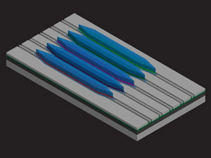
Fabricating a quantum cascade laser on silicon was a challenging task made more difficult by the fact that silicon dioxide becomes heavily absorptive at longer wavelengths in the mid-infrared. "Not only did we have to build a different type of laser on silicon, we had to build a different silicon waveguide too," says Spott. "We built a type of waveguide called a SONOI waveguide [silicon-on-nitride-on-insulator], which uses a layer of silicon nitride [SiN] underneath the silicon waveguide, rather than just SiO2."
 Picture: 3D artistic depiction of multiple quantum cascade lasers integrated above silicon waveguides. Credit: Alexander Spott.
The development could lead to several applications. "Traditionally, silicon photonic devices operate at near-infrared wavelengths, with applications in data transmission and telecommunications," Spott says. "However, there is emerging research interest in building these silicon photonic devices for longer mid-infrared wavelengths, for a range of sensing and detection applications, such as chemical bond spectroscopy, gas sensing, astronomy, oceanographic sensing, thermal imaging, explosive detection, and free-space communications," he adds.
The next step for the team is to improve the heat dissipation to improve the performance of the QCLs and to allow them to make continuous-wave (cw) QCLs on silicon. "We generally hope to improve the design to get higher powers and efficiency," Spott says. "This brings us closer to building fully integrated mid-infrared devices on a silicon chip, such as spectrometers or gas sensors," he adds. "Silicon is inexpensive, the fabrication can be scaled up to significantly reduce the cost of individual chips, and many small devices can be built on the same silicon chip – for example, multiple different types of sensors operating at different mid-infrared wavelengths."
A paper 'Quantum Cascade Laser on Silicon at 4.8 μm' by Alexander Spott, Jon Peters, Michael Davenport, Eric Stanton, Charles Merritt, William Bewley, Igor Vurgaftman, Jerry Meyer, Jeremy Kirch, Luke Mawst, Dan Botez and John Bowers will be presented at the Conference on Lasers and Electro-Optics (CLEO 2016) on 9 June (2-4pm) in the San Jose Convention Center, San Jose, CA, USA.
Mid-infrared quantum cascade laser III-Vs-on-Si Direct wafer bonding silicon photonics
https://labs.chem.ucsb.edu/bowers


