


- News
9 August 2016
Chemical lift-off of full-wafer gallium nitride with zinc oxide interlayer
Researchers based in UK, France, Australia and the USA have developed a chemical epitaxial lift-off (ELO) technique for full 2-inch-diameter gallium nitride (GaN) grown on sapphire and free-standing substrates [Akhil Rajan et al, J. Phys. D: Appl. Phys., vol49, p315105, 2016]. The method used a sacrificial zinc oxide (ZnO) interlayer. The researchers hope that the ELO technique could result in better quality material, and hence higher efficiency, for light-emitting diodes and other GaN applications.
"The high optical quality of the lifted GaN suggests that ELO might offer the possibility, in the future, of transferring full wafers of GaN devices from the expensive GaN substrate to alternative substrates and then reclaiming/recycling the expensive GaN substrate for future use," comments the team from Heriot-Watt University in the UK, Nanovation in France, University of Technology Sydney in Australia, Georgiatech-CNRS in France, Georgia Institute of Technology/GT-Lorraine in France, Northwestern University in the USA, University of Nottingham in the UK, Génie électrique et électronique de Paris (GeePs) in France, and Université Versailles Saint Quentin in France
The researchers add: "Furthermore, our experience with laser lift-off of thicker GaN layers suggests that they would be self-supporting. As a next step it is thus envisaged to do ELO with thicker layers in order to test if it is possible to avoid using the host-bonding step."
The 140nm GaN epitaxial lift-off (ELO) layers were grown on 2-inch-diameter ZnO on free-standing GaN and on c-Al2O3 sapphire substrates. The ZnO layer thicknesses were 260nm on GaN and 160nm on c-Al2O3. The GaN substrate was bought from Lumilog, which uses hydride vapor phase epitaxy (HVPE) to produce free-standing wafers. The threading dislocation density of the Lumilog wafer was specified at less than 5x10⁶/cm2. Typical heteroepitaxy of GaN on sapphire results in threading dislocation densities of at least 107/cm2 and more usually in the range 108/cm2-109/cm2.
The ZnO layers were grown by pulsed laser deposition of zinc in an oxygen atmosphere. The GaN epilayer was deposited using low-pressure, low-temperature metal-organic vapor phase epitaxy (MOVPE). The low pressure and temperature were designed to combat the ZnO dissociation that normally occurs in MOVPE of GaN on such material. The GaN nitrogen precursors were ammonia with added dimethylhydrazine (C2H8N2) in nitrogen carrier. The dimethylhydrazine was used to enhance nitrogen concentrations.
The ELO used an Apiezon W wax host with a glass superstrate providing rigidity to avoid cracking, curling and break-up from strain release (Figure 1). The lift-off separation occurred using hydrochloric acid to dissolve the ZnO sacrificial layer. Near the edge, the ZnO etch rate was more than 1mm per hour, but this slowed to 0.5mm per hour towards the center.
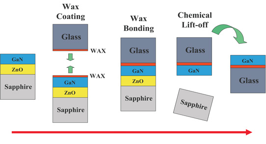
Figure 1: Wide-area chemical lift-off process flow.
X-ray analysis suggested that the GaN grown on free-standing GaN had "a significant reduction in crystallographic dispersion relative to typical GaN layers grown on ZnO/sapphire," according to the researchers.
The researchers report: "After lift-off, the substrates and the GaN layers all showed mirror-like surfaces although there was some cracking in the lifted GaN layers in regions where the wax did not bond the GaN layers to the glass host."
X-ray analysis of the ELO GaN gave broader peaks for material grown on free-standing GaN, compared with that grown on c-Al2O3. "This is not as would be expected from the increased grain size in the layer grown on GaN and film thickness effects should be negligible because the layers are approximately the same thickness," the researchers comment. The reason for the broadening after lift-off was unclear. One possibility raised is curling of the GaN from imperfect bonding of the wax to the glass.
However, cathodoluminescence (electron-beam excitation) studies at 8.5K on the ELO GaN from the free-standing GaN substrate showed near-band-edge peaks attributed to donor bound excitons (DX), and both zero phonon and single phonon donor-acceptor pair (DAP and DAP-LO) transitions at 3.33eV, 3.25eV and 3.16eV, respectively (Figure 2). The researchers add: "The presence of both excitonic emission and a phonon replica peak in this sample indicates that the growth on a GaN substrate led to a higher-quality GaN film than the growth on a sapphire substrate."
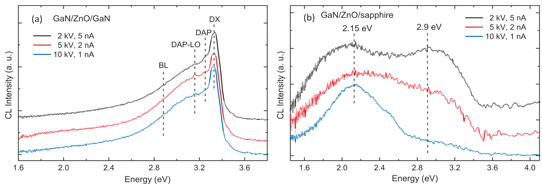
Figure 2: Depth-resolved cathodoluminescence spectra of GaN at 85K after lift-off from (a) GaN and (b) c-Al2O3 sapphire substrates and subsequent bonding to glass. Spectra are shifted vertically for clarity.
The response from the material grown on c-Al2O3 was broad blue (~2.9eV) and yellow (~2.15eV) lines and no near band-edge emission. It is suggested that the blue line was from zinc substitution in the GaN lattice at a level below the 1000 parts-per-million detection limit of energy-dispersive x-ray spectroscopy, which had found no detectable zinc. The yellow lines were probably due to carbon impurities. The zinc level was higher near the surface – the position where the ZnO/GaN interface was in the original growth before ELO.
Chemical epitaxial lift-off ELO GaN ZnO
http://dx.doi.org/10.1088/0022-3727/49/31/315105
The author Mike Cooke is a freelance technology journalist who has worked in the semiconductor and advanced technology sectors since 1997.


