


- News
17 August 2016
Wafer reclaim for indium gallium aluminium phosphide light emission
Researchers in Germany have been developing an epitaxial lift-off (ELO) process that would allow gallium arsenide (GaAs) substrates to be reused for indium gallium aluminium phosphide (InGaAlP) thin-film light-emitting diode (LED) production without expensive and time-consuming grinding and polishing [M. Englhard et al, J. Appl. Phys., vol120, p045301, 2016].
Osram Opto Semiconductors GmbH was the main contributor to the research, with other researchers associated with Leibniz-Institut für innovative Mikroelektronik (Innovations for High Performance Microelectronics, IHP), Brandenburg University of Technology (BTU) Cottbus-Senftenberg.
The team writes: "These investigations can help by improving the ELO technique to reduce costs for GaAs substrates and reduce toxic arsenic waste. Expensive grinding or polishing processes are not necessary after ELO."
The proposed ELO process would use a sequence of layers that consisted of In0.5(Ga0.45Al0.55)0.5P (labeled as 'Q55') on the GaAs substrate, and GaAs layers sandwiching a selective-etch sacrificial layer such as AlAs (Figure 1). "This process would result in reducing costs for LEDs and reducing much arsenic waste for the benefit of a green semiconductor production," the team writes.
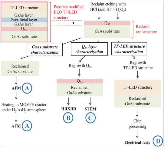
Figure 1: Schematic overview of different process steps to characterize quality of GaAs substrate after reclaim etching.
The Q55 layer is used to protect the GaAs substrate for reuse. The GaAs layers of the sandwich prevent damage to the Q55 and thin-film LED layers during sacrificial layer selective etch.
Normal thin-film InGaAlP LED production consists of growth on GaAs, bonding to a hard carrier wafer, and destructive removal of the GaAs growth substrate by grinding, polishing or etch. The toxic waste, including arsenic, is expensive to recycle. Even reclaiming the GaAs substrate with present ELO techniques involves grinding and polishing to achieve a suitable reconditioned surface for growth of further thin-film LEDs.
The researchers focused on confirming that the Q55 layer removal resulted in a suitable GaAs surface for re-growth of thin-film LEDs on the reclaimed GaAs substrate. The Q55 layer was pseudomorphically grown by metal-organic vapor phase epitaxy (MOVPE) on 4-inch 6°-offcut GaAs at 660°C. The GaAs and Q55 layer are lattice matched at 784°C, so the growth is under slightly mismatched conditions. The reclaim etch resulted in a flat surface with ~0.2nm root-mean-square (rms) roughness.
The thin-film LEDs grown on various reclaimed wafers had similar performance to devices grown on reference substrates. The median forward voltage for all devices produced on reference or reclaimed wafers was 2.17V. The median center wavelength and optical intensity were 626nm (orange) and 1794mCd, respectively.
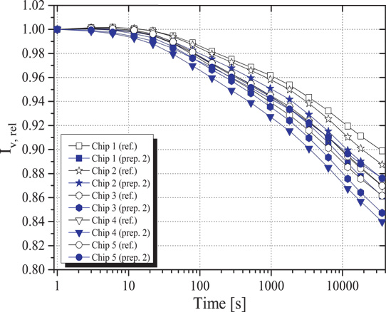
Figure 2: Typical relative luminous intensity (Iv,rel) degradation with time of chips on Ge-carrier in overstress testing of devices grown on reclaimed and reference wafers.
The researchers also carried out high-temperature/current stress testing. The team claims good performance for the thin-film LEDs under stress. There was a "small inhomogeneity of the chips" attributed to process-related fluctuations. To my view, however, the presented graph (Figure 2) suggests that the chips grown on the reused substrates tend to be slightly less robust than the reference.
Epitaxial lift-off GaAs substrates InGaAlP LEDs
http://dx.doi.org/10.1063/1.4955333
The author Mike Cooke is a freelance technology journalist who has worked in the semiconductor and advanced technology sectors since 1997.


