


- News
3 August 2016
Boosting hole injection by including indium gallium nitride in p-contact
China's South China University of Technology and Taiyuan University of Technology have developed a p-contact layer for indium gallium nitride (InGaN) light-emitting diodes (LEDs) with improved hole injection [Zhiting Lin et al, J. Phys. D: Appl. Phys., vol49, 285106, 2016]. The researchers designed a two-layer p-contact consisting of p-GaN and p-In0.05Ga0.95N that increased light output power by almost 40% at 75mA injection and wall-plug efficiency (WPE) by 26.0%.
Hole injection is a particular problem in InGaN and other III-nitride LEDs since p-type doping is conventionally achieved with magnesium that has an acceptor level a couple of hundred meV (~180meV) above the GaN valence band. Doping for electron-majority n-type material is usually achieved with silicon, where the donor level is ~15meV below the GaN conduction band. The disparity leads to an imbalance of carrier injection into the active region where it is hoped the electrons and holes will recombine as photons. The imbalance causes non-radiative recombination and other losses such as electron overshoot into the p-GaN contacts.
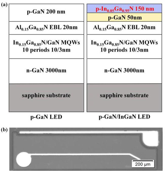
Figure 1: (a) Structures of p-GaN and p-GaN/p-InGaN LEDs and (b) optical microscope image of LED chip.
Two LED samples were created – one a traditional LED wafer with p-GaN contact and the other with a combination of 50nm p-GaN and 150nm p-InGaN (Figure 1). The materials were grown by metal-organic chemical vapor deposition (MOCVD) on sapphire. The fabricated devices were conventional lateral LEDs with plasma etched mesas, 250nm indium tin oxide (ITO) transparent conductive p-electrode, and chromium/platinum/gold contact pads. The chip areas were 750μmx220μm.
In actual electroluminescence experiments (Figure 2), the p-GaN/p-InGaN LED showed a 39.4% increase over the pure p-GaN device in light output power at 75mA injection (83.2mW/59.7mW = 1.394).
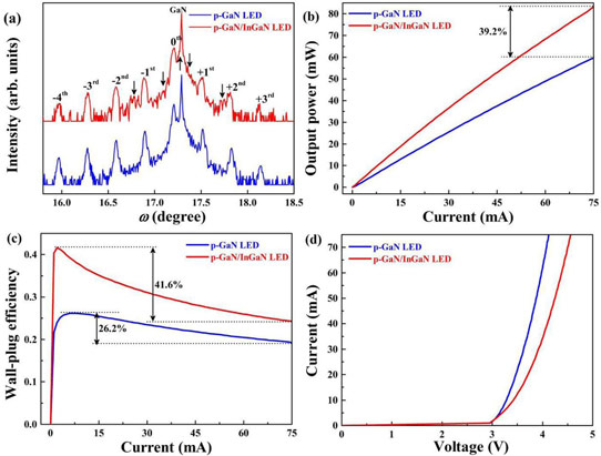
Figure 2: Comparisons of p-GaN and p-GaN/p-InGaN LED wafers and LED chips: (a) high-resolution x-ray diffraction ω − 2θ symmetrical (0002) scans; (b) light output power; (c) wall-plug efficiency; and (d) current versus voltage curves.
The droop in WPE was 26.2% from the peak for the pure p-GaN LED, compared with 41.6% for p-GaN/p-InGaN. However, the WPE peak was lower for the pure p-GaN LED and the p-GaN/p-InGaN maintained higher WPE values through to 75mA. At 75mA, the WPE of the p-GaN/p-InGaN LED was still 26.0% greater than for the pure p-GaN contacted device.
The increased droop for the p-GaN/p-InGaN LED arises from increased resistance at increased current injection. At 20mA, the forward voltage was 3.46V for a pure p-GaN contact and 3.71V for p-GaN/p-InGaN.
The researchers comment: "The increasing electric resistance could result from the fact that the thick p-InGaN layer might relax on the p-GaN layer and thus crystalline defects are generated in the p-InGaN layer. These crystalline defects serve as scattering centers, resulting in reduction of hole mobility."
Simulations suggest that one effect of the p-GaN/p-InGaN contact layer is to increase the electron barrier of the aluminium gallium nitride (AlGaN) electron-blocking layer (EBL), while at the same time reducing the barrier to hole injection. The electron barrier was increased in the models from 489meV for a pure p-GaN contact to 528meV for p-GaN/p-InGaN. The respective hole injection barriers were 318meV and 306meV. EBLs are commonly implemented to confine electrons to the MQW active region, preventing overshoot into the p-GaN contacts.
Another effect suggested by the simulation is the creation of a triangular hole well at the p-GaN/p-InGaN interface. The density of holes in the region of the well is estimated to be 2x10¹⁸/cm3, compared with less than 5x10¹⁶/cm3 for the same position in the pure p-GaN contact layer. The knock-on effect at the EBL interface is an increase in hole density from 2x10¹⁸/cm3 to 6x10¹⁸/cm3.
"This phenomenon means that there are more holes available to inject into the MQW region, which is very similar to the result of increasing acceptor-doping density of GaN-based materials," the team writes.
The result of the increased hole injection with p-GaN/p-InGaN contacts at 100A/cm2 is expected to be a 25% increase in the number of holes in the multiple quantum well (MQW) light-emitting active region. There is also predicted a 10% increase in electron numbers in the MQW. The radiative recombination at 100A/cm2 should also increase by 55%. The simulated droop in internal quantum efficiency (IQE) from the peak value to that at 100A/cm2 is 32.9% for the p-GaN LED and 21.7% for the p-GaN/p-InGaN device.
http://dx.doi.org/10.1088/0022-3727/49/28/285106
The author Mike Cooke is a freelance technology journalist who has worked in the semiconductor and advanced technology sectors since 1997.


