


- News
23 August 2016
Reducing misfit dislocations in green semi-polar light-emitting diodes
University of California Santa Barbara (UCSB) in the USA has used limited-area epitaxy (LAE) on semi-polar gallium nitride (GaN) substrates to reduce misfit dislocation (MD) densities in multiple quantum well (MQW) green light-emitting diode (LED) structures [C. D. Pynn et al, Appl. Phys. Lett., vol109, p041107, 2016].
The effect of greater limiting the area of growth mesas was to improve external quantum efficiency (EQE). At 35A/cm2 injection, the EQE for the most limited-area device with 5μm-wide mesas was 73% higher than for 20μm-wide LAE LEDs.
The researchers point out, however: "Still, the peak EQE of the best devices in this study was approximately an order of magnitude lower than that of previous reported green semi-polar InGaN-based LEDs. We attribute this to a reduction in radiative efficiency due to non-uniform carrier injection across the MQW active region, which likely caused an uneven distribution of electrons and holes near the bottom-most and top-most QWs, respectively. Further optimization of this MQW active region design is needed to mitigate these effects and improve device efficiency."
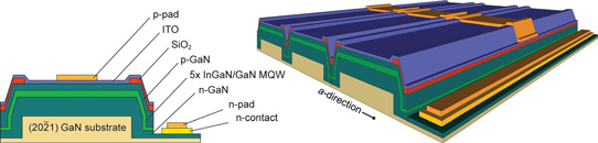
Figure 1: Cross-section and perspective schematics of LAE LED grown and fabricated on patterned substrate.
The MDs that reduce efficiency are caused by lattice mismatch between the underlying GaN substrate and high-indium-content indium gallium nitride (InGaN) needed for green light emission. The strain from mismatch is released by lattice plane slippages that generate MDs, which increase the probability of non-radiative electron-hole recombination and thus reduce efficiency.
To avoid MDs, the strained layers are usually limited below a critical thickness, reducing the active volume of the devices that can emit light.
The LED material was grown by metal-organic chemical vapor deposition (MOCVD) on (2021) GaN substrates from Mitsubishi Chemical Company. The threading dislocation density was ~5x10⁶/cm2.
Substrate patterning for the limited-area epitaxy was achieved by chlorine plasma etch, giving 1μm-high mesas. The mesas were 300μm-long stripes of widths varying between 5μm and 20μm. A series of mesas 300μm wide was created with 2μm separation. The single LEDs consisted of these 300μmx300μm arrays.
The orientation of the mesas was in the c-direction projected in-plane, previous work having determined this as the most effective for preventing the generation of misfit dislocations.
The LED layer structure consisted of a 1μm n-GaN contact, five-period MQW, 8nm p-type aluminium gallium nitride (p-Al0.15Ga0.85N) electron-blocking layer, and 40nm p-GaN contact. The MQW contained 4nm In0.25Ga0.75N wells separated by 4nm GaN barriers.
Silicon dioxide was deposited on the sidewalls of the mesas and 1μm into the top surface to confine current injection. The LED chip was defined by a further 1μm-high mesa etch of the 300μmx300μm array. The p-contact layer was coated with 100nm indium tin oxide (ITO) transparent conducting oxide (TCO) before metal deposition of the titanium/aluminium/nickel/gold n-contact, and titanium/gold n- and p-contact pads.
Light extraction was improved by thinning, polishing and roughening the back-side of the device. The roughening consisted of forming truncated pyramids. The wafer was diced and the single chips mounted on silver headers before encapsulation in silicone.
Fluorescent micrography found that the effect of increasing the mesa strip width was an increase in the number of dark-line defects, indicating stress relaxation via MD formation. There were three types of dark-line defects, suggesting different routes to MDs: one came through basal plane slip and the remainder through non-basal plane slip.
With 5μm mesa width, the basal-plane MD density was reduced, and the non-basal-plane MDs were "completely eliminated", according to the researchers. Non-basal-plane MDs were found to affect light emission from electrical injection more than basal-plane MDs.
The team comments: "The MD density on the 5μm LAE mesas was too low to cause a measurable degree of relaxation, resulting in the nearly coherent growth of an active region with an average composition of In0.12Ga0.88N and a thickness of 40nm that is at least twice the theoretically predicted limit."
The peak electroluminescence wavelength at 35A/cm2 injection was in the range 532-536nm. The reduced mesa width of 5μm gave the highest external quantum efficiency (Figure 2).
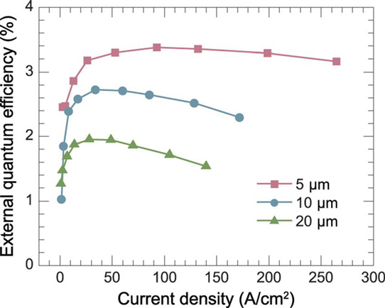
Figure 2: Dependence of EQE on current density for LAE LEDs with 5μm, 10μm and 20μm wide substrate mesas.
In addition to reduced dislocation densities, the researchers suggest that the improved performance of the 5μm LAE LED could be partly due to enhanced light extraction caused by an increased number of mesa sidewalls.
Limited-area epitaxy LAE Semi-polar GaN substrates MQW Green LEDs MOCVD
http://dx.doi.org/10.1063/1.4960001
The author Mike Cooke is a freelance technology journalist who has worked in the semiconductor and advanced technology sectors since 1997.


