


- News
22 August 2016
Gallium arsenide phosphide solar cells on silicon with record 12% efficiency
Yale University and University of Illinois Urbana in the USA have improved the efficiency of gallium arsenide phosphide (GaAsP) solar cells on silicon (Si) by reducing threading dislocation densities (TDDs) [Kevin Nay Yaung et al, Appl. Phys. Lett., vol109, p032107, 2016]. The efficiency under simulated AM1.5G solar illumination of up to 12% is claimed to be among the best reported for uncoated GaAsP solar cells on GaP/Si templates. The researchers quote 9.8% as the previous record.
It is hoped that such cells can be used in tandem with low-cost silicon-based solar cells to compete with much more expensive ~45% high-efficiency multi-junction devices based on compound semiconductor substrates.
The energy bandgap (Eg) of GaAsP can be tuned to the 1.6-1.8eV range, with 68-85% arsenic content, that would be useful as a top cell over silicon (~1.1eV). The GaAsP layers would more efficiently filter out and convert high-energy photons to energy, leaving silicon to handle the longer wavelengths that it is more suitable for.
Previously, TDD levels around 108/cm2 have hampered development of GaAsP solar cell layers on silicon. The Yale/Illinois-Urbana work has reduced this to as low as 4.0x10⁶/cm2. High TDD results in non-radiative recombination and reduced open-circuit voltage (VOC)
The team comments: "We estimate that a well-designed anti-reflection coating with low grid coverage could boost our [short-circuit current density] JSC to ~18mA/cm2 , resulting in a top-cell efficiency of ~16%. If the top-cell efficiency can be increased to 20% while achieving a bottom silicon cell efficiency of ~10%, then a dual-junction efficiency value approaching 30% is attainable."
Even higher efficiencies could result from adding another top junction solar cell based on indium gallium phosphide (InGaP). Such solar cells have already been produced with low TDD and bandgap offset (WOC = Eg/q – VOC, with q electron charge).
The team also suggests that its dislocation engineering could be used to integrate lasers and photoelectrochemical cells on silicon.
The GaAsP solar cell samples were grown on bulk GaP substrates and GaP/Si templates using molecular beam epitaxy (MBE). GaP has a lattice mismatch with silicon of ~0.4% at 300K. The GaP substrate was supplied by ITME of Poland. The GaP/Si was grown by NAsPIII/V GmbH of Germany using metal-organic chemical vapor deposition (MOCVD) on (001) p-Si (Figure 1).
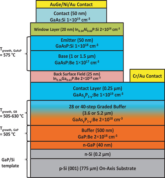
Figure 1: Schematic of GaAsP/GaP/Si solar cell layer structure.
Beryllium (Be) provided p-type doping for the MBE GaAsP buffer/contact/base and indium gallium phosphide (InGaP) back surface field layers. The n-type doping was provided by silicon for the MBE GaAsP emitter/contact and indium aluminium phosphide (InAlP) window layers.
The solar cell structures were fabricated with wet mesa etching and metal top contacts. There was no anti-reflective coating.
Before growing the solar cell, the researchers optimized the growth temperature by depositing thick GaP buffers on a GaP/Si template and studying the effect on threading dislocation density. The optimum temperature was found to be 505°C. Low-TDD buffer layers tend to result in better quality subsequent epitaxial layers.
The TDD increased below and above the 505°C value. The researchers believe the low-temperature increase (2x at 410°C) was due to reduction in the amount of dislocation glide. Dislocation glide is thought to relax strain, sweeping away the dislocations and thus reducing TDD. The high-temperature TDD increase (3x at 695°C) was attributed to nucleation of new dislocations.
Further reduction in TDD was achieved by lowering the growth rate at 505°C to allow more time for dislocation glide to act. However, increased growth time could also enhance dislocation nucleation at higher temperature.
Table 1: Summary of device parameters of GaAsP solar cells grown on GaP/Si templates. GaP growth was fixed at 505°C. Highest efficiency and lowest TDD were for graded barriers grown in the range 555°C–600°C (TGB).
| TGB [°C] | Grading rate [%/μm] | Eg [eV] | VOC [V] | WOC [V] | JSC [mA/cm2] | FF | TDD [x106/cm2] | Efficiency [%] |
| 505 | 0.80 | 1.69 | 1.05 | 0.64 | 12.7 | 0.76 | 27.5 | 10.2 |
| 555 | 0.80 | 1.71 | 1.13 | 0.58 | 12.4 | 0.80 | 5.1 | 11.2 |
| 575 | 0.80 | 1.69 | 1.12 | 0.58 | 12.7 | 0.77 | 6.0 | 10.9 |
| 575 | 0.56 | 1.69 | 1.15 | 0.54 | 13.1 | 0.76 | 4.6 | 11.5 |
| 575 | 0.38 | 1.70 | 1.15 | 0.55 | 13.3 | 0.79 | 4.2 | 12.0 |
| 600 | 0.80 | 1.70 | 1.15 | 0.55 | 13.2 | 0.78 | 5.3 | 11.8 |
| 600 | 0.56 | 1.69 | 1.13 | 0.56 | 12.0 | 0.80 | 4.0 | 10.9 |
| 630 | 0.80 | 1.69 | 1.11 | 0.58 | 11.9 | 0.78 | 7.8 | 10.3 |
The graded buffer (GB) layers with lower TDD were grown at temperatures in the range 575°C-600°C. Also, the grading rate was again important with lower TDD achieved at 575°C and 600°C when the rate was reduced from 0.8%/micron to 0.56%/μm (Table 1). A smaller reduction in TDD was gained by reduction of the grading to 0.38%/μm at 575°C. Of course, reducing the grading rate increases production time and cost.
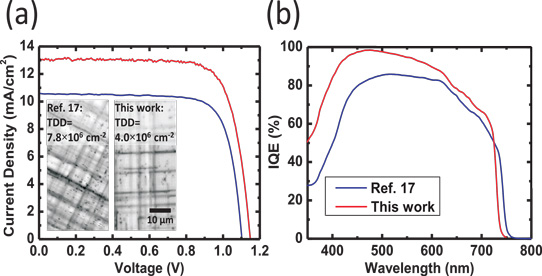
Figure 2: Comparison of GaAsP/GaP/Si solar cell (a) current density versus voltage curves with electron beam-induced current (EBIC) images inset and (b) IQE characteristics with group's latest (red, top line) and previous work (blue, bottom line).
Comparing one of the better devices produced with the group's previous work (Figure 2), the researchers comment: "While the improvement in short-wavelength [internal quantum efficiency] IQE shown in [Figure 2(b)] results from a thinner emitter and higher-Eg window, we believe that the improvement in IQE near the band-edge largely results from lower TDD and higher electron lifetime in the base. Taken together, these performance boosts have enabled us to achieve GaAsP on GaP/Si solar cell efficiencies (without anti-reflection coatings) above 11.5%, surpassing the previously published record of 9.8%."
GaAsP solar cells GaAsP MBE MOCVD
http://dx.doi.org/10.1063/1.4959825
The author Mike Cooke is a freelance technology journalist who has worked in the semiconductor and advanced technology sectors since 1997.


