


- News
29 December 2016
Non-polar aluminium gallium nitride from two-way pulsed precursor flow
Researchers at Southeast University and Changshu Institute of Technology in China have improved the crystal quality of a-plane aluminium gallium nitride (AlGaN) with Al content more than 60% grown by metal-organic chemical vapor deposition (MOCVD) on r-plane sapphire [Jianguo Zhao et al, Appl. Phys. Express, vol10, p011002, 2017]. The team used a technique that used separate pulses of nitrogen and aluminium precursors to avoid parasitic chemical reactions that reduce aluminium incorporation in the crystal structure.
High-Al-content AlGaN is used to create deep ultraviolet light-emitting diodes (DUV LEDs) with wavelengths shorter than 300nm. Such devices are being developed for killing dangerous micro-organisms in water and air for disinfection/purification purposes.
Presently the efficiency of DUV LEDs is pitifully low – of the order of a few percent. One source of inefficiency is that standard growth techniques result in c-plane material with electric fields from charge polarization effects that reduce electron-hole overlap, hindering recombination into photons. The problem is commonly referred to as the quantum-confined Stark effect. It can be reduced or eliminated by using non-polar or semi-polar III-nitride semiconductor heterostructures. The a-plane (11-20) is an example of a non-polar crystal structure orientation.
Other inefficiencies for c-plane devices are added by optical anisotropy and energy band structure effects. However, the growth of a-plane material is challenged by a large lattice-mismatch with r-plane sapphire, basal stacking fault tendencies, and the strong anisotropy of such epilayers.
The a-plane (11-20) AlGaN growth was carried out at 40Torr low pressure. The respective precursors for Al, Ga, silicon and nitrogen were trimethylaluminum (TMAl), trimethylgallium (TMGa), silane (SiH4), and ammonia (NH3).
The growth sequence on r-plane (2-204) sapphire was surface contamination removal at 1060°C in hydrogen, 20nm 600°C AlN nucleation, 1100°C AlN buffer, and 800nm AlGaN epitaxial layer. The buffer was grown either continuously or in pulse-flow mode. Various AlGaN layer growth processes were tested: continuous (sample A), pulsed-flow (B), and two-way pulsed-flow (C).
The sample B method involved pulses in the ammonia flow only, for both the AlN buffer and AlGaN epilayer. Sample C was grown with pulses of ammonia and TMAl organized to suppress parasitic gas-phase reactions between these components. At the same time, the TMGa flow was continuous. The precursor pulses in all cases lasted 6 seconds.
X-ray analysis suggested that the Al content of the AlGaN epilayers was 60%, 66% and 68% for samples A to C, respectively. The researchers attribute the higher Al content in samples B and C to suppression of the parasitic gas-phase reactions between ammonia and TMAl, enhancing Al incorporation.
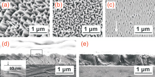
Figure 1: Top-view surface SEM micrographs for samples (a) A, (b) B and (c) C with white arrows pointing in c-direction; and cross-sectional SEM micrographs for samples (d) A and (e) C.
Scanning electron microscope inspection of the surface showed that sample C had much reduced roughness with large defect-free areas compared with the other samples. The researchers comment: "In fact, both large and small pyramidal defects coalesced very well, and the penetration depth of the defects into the epilayer was found to be very shallow for sample C, resulting in an apparent reduction in defect density, as demonstrated by the top-view surface and cross-section SEM micrographs" (Figure 1). The team adds: "This improvement in crystalline quality for the non-polar a-plane AlGaN epi-layer is the result of the introduction of the innovative two-way pulsed-flow growth technology, which can be explained based on the fact that there is more time for the Al adatoms to migrate to their appropriate lattice sites under an Al-rich growth condition."
Atomic force microscope (AFM) scans also showed reduced root-mean-square (RMS) roughness for sample C (Figure 2). In 10μmx10μm scans the RMS roughness values corresponding to samples A to C were, in order, 15.37nm, 6.94nm and 2.02nm.
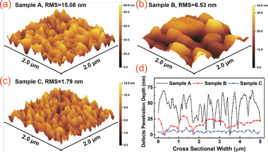
Figure 2: AFM three-dimensional view images and RMS values measured within detection area of 2μmx2μm for samples (a) A, (b) B and (c) C; and (d) AFM cross-sectional graphs for samples A (black dotted line), B (solid red line), and C (solid blue line).
Sample C also showed increased transmittance of light, especially when the wavelength was longer than 400nm. The peak enhancement was 36.4% in the 200-400nm range. The researchers comment: "This improvement in light transmission characteristics was attributed to the smoothed surface morphology and the improved crystalline quality for the sample grown using the innovative two-way pulsed-flow technology. It is well known that smaller RMS values and lower defect densities correlate with less absorption, which is of critical importance for enhancing the light extraction efficiency of DUV-LEDs."
The higher Al content of sample C resulted in an absorption edge 8nm shorter in wavelength (higher energy bandgap) than sample A.
https://doi.org/10.7567/APEX.10.011002
The author Mike Cooke is a freelance technology journalist who has worked in the semiconductor and advanced technology sectors since 1997.


