


- News
12 December 2016
Heterogeneous integration of 2.3μm DFB laser diodes on silicon photonics
Researchers based in Belgium and Germany have produced ~2.3μm-wavelength distributed feedback (DFB) laser diodes on a silicon photonics integrated circuit (PIC) [Ruijun Wang et al, Appl. Phys. Lett., vol109, p221111, 2016]. The team from Ghent University-imec and Ghent University in Belgium and Technische Universität München in Germany see potential for compact integrated spectroscopic sensors. The researchers demonstrated the use of their device in a tunable diode laser absorption spectroscopy (TDLAS) experiment using carbon monoxide gas. Further, many important gases have narrow, dense absorption lines in the 2-3μm wavelength range.
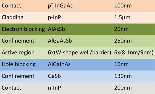
Figure 1: III-V gain section.
The assembly consisted of a III-V gain section (Figure 1) over a silicon distributed feedback (DFB) grating and III-V/silicon spot-size converters (SSCs, Figure 2). The gain section was produced by molecular beam epitaxy (ME) on n-type indium phosphide (n-InP). The active region consisted of six W-shaped wells separated by 9nm tensile-strained GaAs0.58Sb0.42 layers. The wells confined holes in a central 2.9nm GaAs0.33Sb0.67 layer, while the electrons were confined either side in two 2.6nm In0.68Ga0.32As layers.
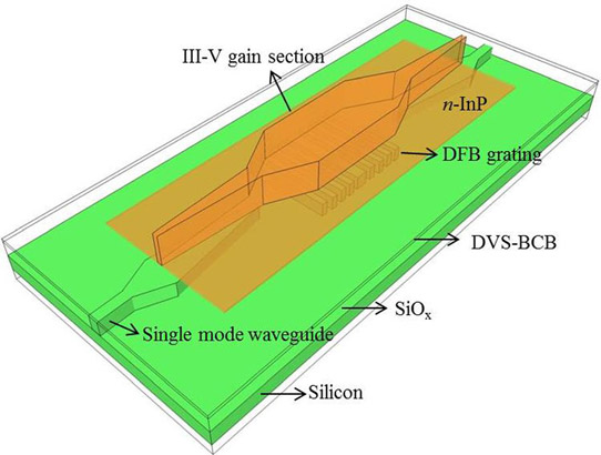
Figure 2: Three-dimensional schematic view of heterogeneously integrated DFB laser.
The III-V mesa was 1000μm long and 5μm wide. The mesa width was chosen to give low waveguide propagation loss and high optical confinement in the III-V active region.
The III-V material was bonded to the silicon with 60nm divinylsiloxane-bis-benzocyclobutene (DVS-BCB) adhesive, giving a calculated 10.1% confinement factor of the transverse electric (TE) fundamental mode in the quantum wells. The tail of the optical mode interacted with the underlying DFB grating, setting the emission wavelength. The DFB consisted of 180nm deep trenches dry etched in the 400nm silicon device layer. The structures were then filled with silicon dioxide and planarized by chemical mechanical polishing (CMP).
The SSCs were realized through tapering both the III-V structure (5μm to 1.2μm over 50μm, and then down to 0.5μm) and underlying silicon (0.2μm to 3μm in 180μm) waveguides. Simulations suggested that such a structure would have more than 90% coupling efficiency.
The silicon PIC processing was performed on IMEC's CMOS pilot line on 200mm silicon-on-insulator (SOI) wafers with 400nm device layer on 2μm buried oxide insulator. The bonding of the III-V material was followed by removal of the InP growth substrate by hydrochloric acid wet etch. The DFB laser structure was then processed with ultraviolet lithography of a silicon nitride hard mask and anisotropic hydrochloric acid etch.
The structure was passivated with DVS-BCB, after which nickel/germanium/gold and titanium/gold were deposited as n- and p-contacts, respectively.
The DFB grating was produced with two periods – 348nm and 353nm, giving lasers '1' and '2', respectively. The devices had corresponding continuous wave (CW) threshold currents of 90mA and 102mA at 5°C, which translate into densities as 1.8kA/cm2 and 2.04kA/cm2. The researchers point out that these values are lower than the first demonstrated 'W'-shaped InGaAs/GaAsSb quantum well lasers grown on InP substrates that gave threshold current densities of 3.2kA/cm2 at 0°C.
The 5°C output power was 1.3mW for Laser 1 and 0.8mW for Laser 2. The researchers comment: "The lower threshold current and higher output power of Laser1 can be attributed to the gain at the lasing wavelength of Laser 1 being higher than that of Laser 2 at 5°C."
At higher temperature, the gain spectrum shifts to longer wavelength, reversing the performance. At 15°C, the output power of Laser 2 was higher than that of Laser 1. The maximum for CW lasing performance was around 17°C for both devices.
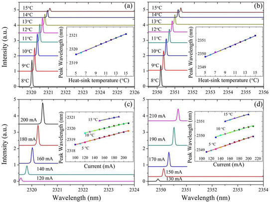
Figure 3: Evolution of lasing spectra as function of heat-sink temperature for DFB grating periods of 348nm (a) and 353nm (b), with both devices biased at 190mA. Inset: dependence of lasing wavelength on temperature; (c) and (d): Emission wavelength versus injection current at heat-sink temperature of 10°C. Inset: wavelength versus injected current at 5°C, 10°C and 15°C.
The researchers suggest that threshold currents and operating temperatures could be improved by reducing thermal resistance by making the DVS-BCB layer thinner, along with connecting the top p-contact to the silicon substrate. Electrically, the series resistance (and resultant Joule heating) could be reduced by optimizing metallization processes.
At 10°C and 190mA current, the peak wavelength was 2320nm for Laser 1 and 2350nm for Laser 2. The lasing was single-mode with 40dB side-mode suppression ratio. The ratio was better than 35dB over the current range 120-210mA. At 5°C the suppression was more than 43dB. The researchers suggest that, by changing the DFB pitch to give different peak wavelengths, an array of lasers could be used for monitoring several gases using a single III–V epitaxial layer stack.
Varying the temperature shifts the wavelength at the rate ~0.15nm/°C due to changes in the effective refractive index of the DFB lasers. The current also changes the wavelength with a rate of 0.01nm/mA.
As a demonstration, the researchers performed spectroscopy on carbon monoxide gas at 740Torr using Laser 1 as the light source at 13°C. The absorption by CO in a gas cell was sensed and the spectrum derived from the current-wavelength relation. The experimental spectrum closely matched the reference form from the High Resolution Transmission (HITRAN) database [https://www.cfa.harvard.edu/hitran/].
DFB laser diodes Silicon photonics GaAsSb
http://dx.doi.org/10.1063/1.4971350
The author Mike Cooke is a freelance technology journalist who has worked in the semiconductor and advanced technology sectors since 1997.


