


- News
21 December 2016
Metal-organic vapor phase epitaxy of nitrogen-polar gallium nitride
Southeast University and Changshu Institute of Technology, both of China, have jointly developed a metal-organic vapor phase epitaxy (MOVPE) process for nitrogen-polar (N-polar) gallium nitride (GaN) with improved crystal quality [Heng Zhang et al, Jpn. J. Appl. Phys., vol56, p015501, 2017]. The researchers call the technique 'reformed-flow-rate-modulation epitaxy', which was performed to create the nucleation layer.
N-polar GaN is usually produced by molecular beam epitaxy (MBE) methods, but MOVPE is the preferred manufacturing technology. MOVPE usually results in Ga-polar GaN.
The N-polar orientation of the crystal structure could be used to improve features of light-emitting structures, such as creating electron-blocking layers with reduced barriers to hole injection using charge-polarization engineering. The technology could also be used to increase options for high-frequency and high-power electronics, where charge polarization is used to create two-dimensional electron gases (2DEG).
The MOVPE was carried out on (0001) sapphire at low pressure (70Torr) with trimethylgallium (TMG) and ammonia (NH3) precursors in hydrogen carrier gas. The process began with the removal of surface contamination at 1060°C and a 30-second nitridation in NH3 at 980°C.
The reformed flow-rate modulation nucleation layer consisted of material grown from 12-second pulses of TMG flow separated by various gaps. Ammonia was supplied continuously throughout the growth. Conventional flow-rate modulation alternates precursors, but GaN tends to decompose in the absence of NH3.
The grown layers consisted of 1070°C 500nm N-polar GaN on top of 600°C 20nm low-temperature (LT) GaN nucleation. The N-polarity of the resulting material was confirmed by potassium hydroxide etching, which preferentially consumes N-polarity material compared with Ga-polarity.
The x-ray rocking curve (XRC) full-width at half maximum (FWHM) was least for an interruption time of 4 seconds between the 12-second pulses of TMG during nucleation growth (Figure 1). Low FWHM values indicate better crystal quality. The different nucleation growth processes had little effect on the total growth time for the N-polar GaN material.
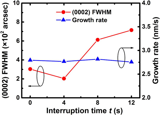
Figure 1: FWHM of XRCs and growth rates as function of TMG-supplying interruption time for N-polar GaN epitaxial layers with LT-GaN nucleation layers grown by reformed flow-rate-modulation technology.
Room-temperature photoluminescence intensity achieved the same optimum of 4-second interruption time (Figure 2). Also, the ratio of band-edge (BE ~364nm) over 'blue-band' (BB ~470nm) emission was highest with 4-seconds-interruption growth.
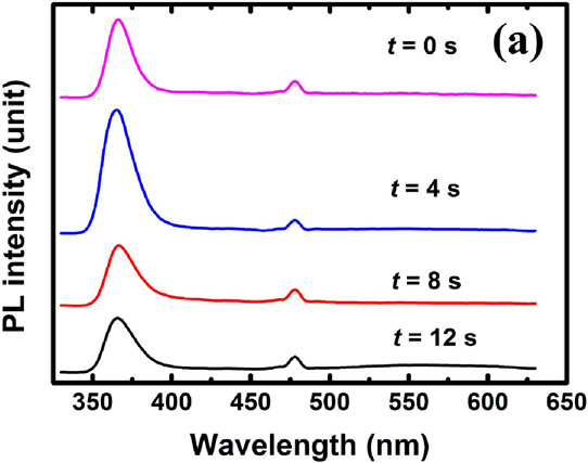
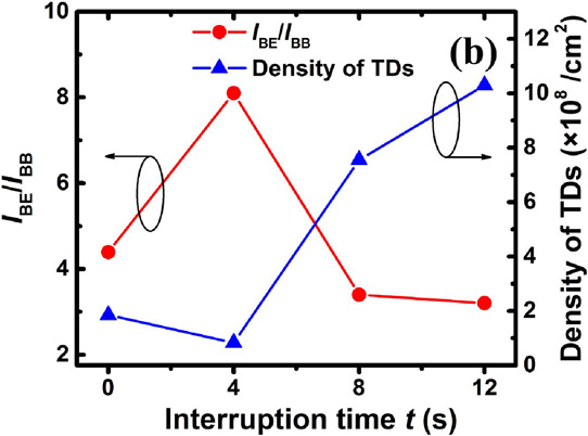
Figure 2: Room-temperature photoluminescence spectra (a), and ratio of intensities, IBE/IBB and density of TDs as function of TMG-supplying interruption time.
The researchers comment; "Since the migration length of the Ga atom is quite long on the surface of (0001)-plane GaN, and the Ga atom usually does not have sufficient time to sit at the lattice site where it should be, the formation of the native Ga vacancy in GaN epitaxial layer was considered to be responsible for the BB emission."
There were few 'yellow-band' (~580nm) emissions, which are often associated with threading dislocations and carbon impurities.
The threading dislocation (TD) density derived from the XRC FWHM measurements was also lowest with 4 seconds interruption between pulses. The story was repeated in Hall measurements, with the lowest intrinsic electron concentration (~4x10¹⁸/cm3) and highest mobility (~90cm2/V-s) occurring in the 4-second sample.
High background carrier concentrations are associated with unintentionally doped oxygen and carbon impurities and acceptor states around TDs. The researchers suggest that the low intrinsic electron concentration was due to the reduction in TDs in the 4-second sample. "Besides, with the successful suppression of the incorporation of oxygen and carbon impurities, the mobility of sheet carriers can be enhanced with the reformed flow-rate-modulation technology owing to a lower ionized impurity scattering," they add.
Atomic force microscopy on the nucleation layer showed a steady increase in root-mean-square (RMS) roughness from no interruption (0.25nm) to 12-seconds (7.89nm). The 4-second sample had a roughness of 0.48nm.
The researchers comment: "With continuous supply of NH3 in our reformed flow-rate-modulation epitaxial growth process, the effects of the decomposition and re-deposition are more notable, leading to a rougher surface morphology. The facts above imply that, just like the role of patterned sapphire substrate (PSS), the shape and dimension of LT-GaN nucleation islands are of crucial importance for achieving high-crystalline-quality N-polar GaN epitaxial layer, and the optimal RMS value for the LT-GaN nucleation island height is 0.48nm."
https://doi.org/10.7567/JJAP.56.015501
The author Mike Cooke is a freelance technology journalist who has worked in the semiconductor and advanced technology sectors since 1997.


