


- News
25 February 2016
Increasing UV electroluminescence from n-ZnO/p-GaN heterojunction
Jilin and Zhengzhou universities in China have increased the electroluminescence (EL) of zinc oxide/gallium nitride (ZnO/GaN) heterojunction light-emitting diodes (LEDs) by growing the crystal layers with oxygen/nitrogen polarities [Junyan Jiang et al, Appl. Phys. Lett., vol108, p063505, 2016].
The change from the more usual zinc/gallium polarity shifts the depletion layer of the p-n GaN-ZnO junction from the interface region into the ZnO, where recombination through excitons can lead to efficient production of ultraviolet (UV) photons. ZnO has a particularly strong ~60meV exciton binding of electron and holes. Also, the direct bandgap is 3.37eV.
The excitons in GaN have binding energies of about 20meV, which is comparable to room-temperature thermal effects (~26meV). ZnO p-n junctions are extremely difficult to realize because p-type material cannot be fabricated in a repeatable/reliable manner. There have been hopes of combining n-ZnO and p-GaN, but usually the electroluminescence is weak or undetectable from the ZnO side.
The LED materials were grown on c-plane sapphire (Al2O3) substrates in an Aixtron CCS 3x2-inch flip-top metal-organic chemical vapor deposition (MOCVD) reactor.
The N-polar p-GaN layer had a hole concentration of 2.4x10¹⁷/cm3. The O-polar n-ZnO layer was produced in a two-step photo-assisted MOCVD process, using diethyl-zinc and oxygen precursors in argon carrier.
The two ZnO steps consisted of a 450°C/6Torr buffer, followed by a 650°C/12Torr 450nm layer. The electron concentration was 2.7x10¹⁷/cm3. Sputtered nickel/gold and gold were used as p-GaN and n-ZnO contacts for the LEDs.
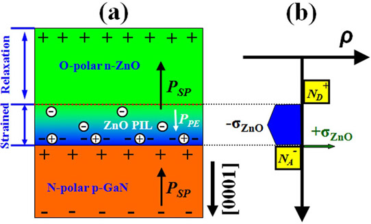
Figure 1: (a) Schematic of O-polar n-ZnO/N-polar p-GaN heterostructure with polarization-induced inversion layer. Fixed charges induced by spontaneous and piezoelectric polarization are also displayed. (b) Spatial distribution of fixed polarization charges and ionized dopants in O-polar n-ZnO/N-polar p-GaN heterostructure.
Naively one expects the depletion region of a p-n junction to be mostly in the region with lowest carrier concentration. However, the chemical bonds of both ZnO and GaN have a large ionic component, resulting in charge polarization effects (Figure 1).
The different polarizations of ZnO and GaN give rise to charge dipole layers at interfaces and electric fields in the bulk of the material. There are both spontaneous and strain-dependent/piezoelectric polarization effects.
The early part of the ZnO layer is under compressive strain due to a 1.8% lattice mismatch with GaN. The compression relaxes later on in the growth. This leads to a polarization interface charge and a distributed charge from the varying strain as the ZnO relaxes.
In O-polar n-ZnO/N-polar p-GaN the depletion layer is shifted into the ZnO layer by a polarization-induced inversion layer. This gives rise to hopes that the electron-hole recombination will occur on the ZnO side, giving highly efficient UV emission based on excitons.
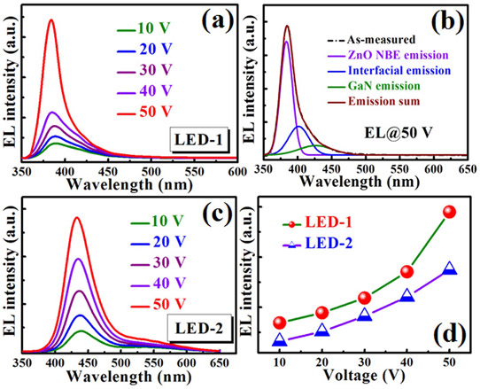
Figure 2: (a) EL spectra of LED-1 (O-polar/N-polar) under various forward bias voltages ranging from 10V to 50V. (b) Gaussian deconvolution of a representative EL spectrum from LED-1 measured at 50V. (c) EL spectra of LED-2 (Zn-polar/Ga-polar) under various forward bias voltages ranging from 10V to 50V. (d) Relationship between integrated EL intensity and voltage of two LEDs.
The LEDs had a turn-on voltage around 3V and demonstrated rectifying behavior. The researchers observed "strong" UV electroluminescence centered at ~385nm (Figure 2). A Gaussian fit of the 50V spectrum gave three peaks at 383nm, 402nm and 430nm.
The researchers associated the strong 383nm UV emission with ZnO near-band-edge (NBE) transitions from free and bound excitons. The 430nm blue emission was attributed to transitions in the p-GaN to the magnesium acceptor level. The researchers add: "The blue emission at 402nm is from the interfacial recombination of the electrons from n-ZnO and the holes from p-GaN."
The researchers also produced a comparison LED-2 with Zn-polar n-ZnO and Ga-polar p-GaN. The p-GaN hole concentration was ~2x10¹⁷/cm3. The EL emission from this device was broad and centered on 435nm (blue). The researchers interpret this as indicating that the depletion region is primarily on the p-GaN side. By contrast, the team believes the depletion region for the O-polar n-ZnO/N-polar p-GaN combination for LED-1 is completely on the ZnO side.
The group comments: "If the PIL of ZnO film is thick enough, the injected electrons and holes could be effectively confined into the ZnO side, producing UV emission from ZnO. More importantly, it is found that the light output power of LED-1 is relatively higher than that of LED-2 under the same test conditions."
At 50V, the O-polar n-ZnO/N-polar p-GaN LED-1 intensity exceeds that of LED-2 by 66%.
The full-width at half maximum (FWHM) of LED-1 became narrower with higher voltage: 48nm at 10V and 24nm at 50V. "As the forward bias changes from 10V to 50V, the intensity of ZnO NBE emission increases much faster than the other two components. And it plays a dominant role when the forward bias is higher than 30V," says the group.
The increasing dominance of the narrow NBE emission reduces the FWHM value.
UV electroluminescence LEDs n-ZnO/p-GaN heterojunction
http://dx.doi.org/10.1063/1.4941230
The author Mike Cooke is a freelance technology journalist who has worked in the semiconductor and advanced technology sectors since 1997.


