


- News
10 February 2016
Hybrid growth of gallium nitride tunnel junctions
University of California Santa Barbara (UCSB) in the USA has been developing a hybrid technique to create III-nitride tunnel junctions (TJs) using a combination of metal-organic chemical vapor deposition (MOCVD) and molecular beam epitaxy (MBE) [Erin C. Young et al, Appl. Phys. Express, vol9, p022102, 2016].
Efficient tunnel junctions could replace indium tin oxide (ITO) current-spreading layers with n-type gallium nitride (GaN) in light-emitting diodes and lasers. Tunnel junctions could also be used in multi-junction solar cells based on III-nitride absorbing layers.
Tunnel junctions are based on flow across very thin depletion layers in p-n junctions. Unfortunately, the wide bandgap of ~3.4eV for GaN leads to relatively large 20nm depletion layers when the doping levels are around 1x10¹⁹/cm3. Such a thick depletion layer chokes off the tunneling current. Increasing the doping level in GaN can be tricky, particular for p-GaN. The difficulties with p-GaN mean that device designs usually place it last in the growth sequence.
Most development of tunnel junctions so far has involved MBE, but MOCVD is the preferred technology in commercial production.
The n-type side of the tunnel junction was grown by ammonia (NH3) MBE on MOCVD GaN p-n and light-emitting diode devices on free-standing semi-polar GaN supplied by Mitsubishi Chemical.
The MBE n-GaN material consisted of a thin heavily doped layer followed by a thicker current-spreading layer. The optimum combination of electrical and optical characteristics – low resistance and high transparency – for the heavily doped layer was found with a carrier concentration of ~1x10²⁰/cm3.
Before MBE the samples were cleaned in solvent. During the 15-minute ramp-up to the 750°C MBE re-growth temperature, the top p-GaN layers were activated. Annealing processes for activating p-GaN generally remove hydrogen, which passivates magnesium doping. Since NH3 was used in the MBE process, it was important to start the re-growth with low ammonia flow to avoid reintroducing hydrogen into the p-GaN interface. The researchers note that the hydrogen level in ammonia MBE is several orders of magnitude lower than that found in MOCVD growth processes.
The team also found that the presence of oxygen at the interface could enhance performance. They comment: "The development of a controllable procedure for introducing oxygen at this interface will be a key to ensuring the repeatability of TJ device characteristics."
The oxygen was detected using atom probe tomography (APT). The researchers comment: "The strong overlap of the Mg and O suggests that a donor–acceptor complex such as ON–2MgGa could have formed at the interface, effectively preventing free surface Mg from incorporating into the n-side of the TJ during regrowth."
Such an effect could lead to a more abrupt drop-off in magnesium concentration, improving the tunneling through the depletion layer.
The material was used to create devices with titanium/gold contacts to the n-GaN material. Reference devices without the tunnel junction were produced with palladium/gold p-contacts. Contacts with ITO were chromium/nickel/gold.
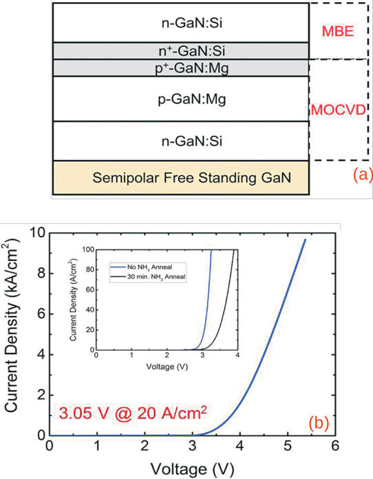
Figure 1: (a) Schematic of test structure with MOCVD p–n diode and re-grown MBE n-GaN. (b) I–V characteristics (a) up to current density of 10kA/cm2, for devices with 25μm radius. Inset: effect of in-situ NH3 annealing prior to MBE re-growth on same devices. Annealed sample showed a higher turn-on voltage and differential resistance compared with unannealed sample.
The researchers created tunnel junction on p-n diodes with total differential resistivity between 7kA/cm2 and 10kA/cm2 of 1.5x10⁻⁴Ω-cm2, including contact resistance (Figure 1). The voltages at 20A/cm2 and 5kA/cm2 were 3.05V and 4.67V, respectively.
The team comments: "We consider this to be among the lowest resistivity and voltage characteristics reported for any III–nitride TJ."
Comparing blue LEDs with tunnel junction and indium tin oxide (ITO) current-spreading layers (Figure 2), the researchers found that the tunnel junction device had a lower voltage of 5.2V at 20mA, compared with 5.87V for the ITO LED. These voltages were on the high side for such devices – the researchers blame unoptimized n-contacts with Schottky, rather than ohmic, behavior.
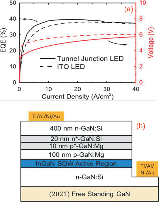
Figure 2: (a) External quantum efficiency and voltage versus current density for TJ LED (solid lines) and ITO reference LED (dotted line) and (b) schematic of TJ LED. Device area was 0.1mm2.
The tunnel-junction LED also had improved external quantum efficiency (EQE) in the low-current range.
http://doi.org/10.7567/APEX.9.022102
The author Mike Cooke is a freelance technology journalist who has worked in the semiconductor and advanced technology sectors since 1997.


