


- News
20 January 2016
Semi-polar gallium nitride on sapphire long-wavelength light-emitting diodes
The UK's University of Sheffield has demonstrated long-wavelength indium gallium nitride (InGaN) single quantum well (SQW) light-emitting diodes (LEDs) on semi-polar (11-22) gallium nitride/sapphire templates [J. Bai et al, Appl. Phys. Lett., vol107, p261103, 2015]. Green to amber devices with peak wavelengths as long as 600nm at 100mA current injection were produced. The researchers describe the electroluminscence as "strong" at 100mA.
Use of sapphire substrates could reduce costs for semi-polar devices. Semi-polar GaN substrates are typically restricted to expensive 10mmx10mm pieces of free-standing or bulk material. Growth of semi-polar GaN on sapphire results in low crystal quality in general.
Semi-polar devices are attractive for longer wavelengths because electric charge polarization of the GaN chemical bond results in large polarization electric fields that inhibit electron-hole recombination to photons in the SQW, reducing efficiency in conventional c-plane LEDs. This is often referred to in the literature as the quantum-confined Stark effect (QCSE).
Growth of devices in semi-polar or non-polar directions reduces the polarization electric field and reduces the quantum efficiency decrease, efficiency droop, and the green and yellow gaps in wavelength coverage associated with QCSEs.
Another advantage of semi-polar material is improved incorporation of indium in InGaN layers. High-indium-content InGaN tends to decompose, with indium evaporation, or segregate into regions of varying compositions, leading to localized states.
The University of Sheffield has developed an overgrowth technique that allows researchers to produce (11-22) GaN on m-plane sapphire. The team sees applications for solid-state lighting and opto-genetics. Yellow light is particularly useful for controlling the activity of genetically modified cells such as neurons.
The Sheffield group notes that previous semi-polar GaN-on-sapphire devices have been limited to blue and green wavelengths. The researchers comment: "Demonstration of yellow or even longer wavelength such as amber semi-polar LEDs with device performance grown on foreign substrates has not yet been reported, as further improvement in growth technologies including crystal quality and enhancing indium incorporation into GaN is requested."
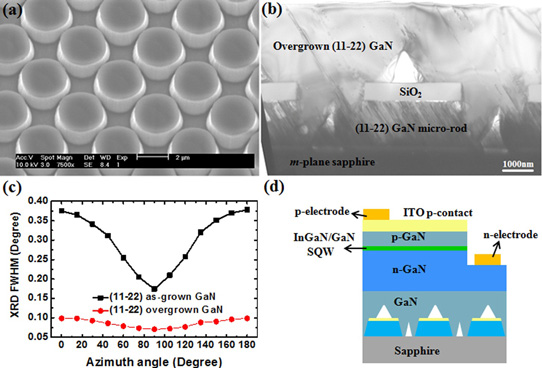
Figure 1: (a) SEM image of micro-rod GaN template; (b) TEM image of (11-22) GaN overgrown on micro-rods; (c) XRD full-widths at half maximum (FWHMs) of overgrown (11-22) GaN and (11-22) GaN template, measured at azimuth angles ranging from 0° to 180°; (d) schematic of (11-22) InGaN SQW LED.
A single layer of (11-22) GaN was grown by metal-organic chemical vapor deposition (MOCVD) on m-plane sapphire using an aluminium nitride (AlN) buffer. The GaN layer was patterned into microrods using photolithographic techniques (Figure 1). The silicon dioxide used as mask was left on top of the GaN micro-rods.
More MOCVD is then carried out to give an overgrown (11-22) GaN template layer about 4μm thick. The silicon dioxide blocks and coalesces defects, reducing dislocation densities to the range 1-4x10⁸/cm2 and basal stacking fault densities to 1-4x10⁴/cm. X-ray analysis suggests that the process results in a crystal quality approaching that for c-plane GaN on sapphire used for the growth of ultra-high-brightness blue LEDs.
InGaN single-quantum-well structures were grown on the templates. The n-GaN and p-GaN layers were 1μm and 150nm, respectively. Lateral LEDs on 0.33mmx0.33mm mesas were fabricated with 100nm indium tin oxide (ITO) transparent conducting p-contact. The n-contact consisted of titanium/aluminium/titanium/gold. The contact pads were titanium/gold.
LEDs with four different color spectra were produced: green, green-yellow, yellow, and amber. As the wavelength of the light increases, the peaks become broader. In the case of the amber LED, the 600nm peak has a shoulder centered on 630nm at 100mA injection. The researchers say that this behavior is indicative of increasing indium separation at the higher compositions needed for longer wavelengths.
The peak wavelength underwent a blue-shift to shorter wavelengths with increasing current. The amount of shift was greatest with the longer-wavelength devices with high indium content. The green, green-yellow and yellow LEDs shifted 8nm, 15nm and 19nm, respectively, between 1mA and 100mA. In c-plane green LEDs the corresponding shift is typically 13nm.
The researchers comment: "This suggests that the quantum-confined Stark effects (QCSEs) in our (11–22) LEDs are effectively suppressed."
The amber devices had an even greater shift that could indicate significant segregation effects with lower-energy localized states being populated at low current injection. These states fill up at higher currents, forcing shorter-wavelength transitions, accounting for the large ~50nm shift. In fact, in the lower-current-injection range less than 20mA, one could consider the LED to be emitting red light (620-740nm).
Problems with fabrication also increased the turn-on voltage of the amber devices (~4V at 20mA). In particular, the p-GaN layer had to be grown at a lower temperature than normal to avoid damage to the InGaN single quantum well. The 20mA voltage for the other devices was in the range 3.0-3.4V, which is standard for InGaN LEDs.
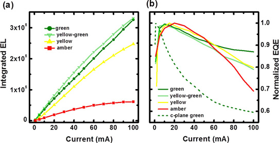
Figure 2: Light output (a) and normalized EQE (b) of the four LEDs as a function of current from 1mA to 100mA. Commercial c-plane green LED (dashed line) reference.
The amber device also suffers from lower light output (Figure 2). All devices have better external quantum efficiency (EQE) performance in terms of droop, compared with commercial c-plane devices. The EQEs at 100mA relative to the maximum were 87%, 80%, 79% and 69% for the corresponding green, green-yellow, yellow and amber devices. The conventional c-plane device in the figure had an EQE at 49% of the maximum (~3mA).
Semi-polar GaN on sapphire LEDs
http://dx.doi.org/10.1063/1.4939132
The author Mike Cooke is a freelance technology journalist who has worked in the semiconductor and advanced technology sectors since 1997.


