


- News
5 July 2016
UK's Artemis facility demonstrates optical control of 2D semiconductor bandgap
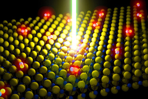 Schematic of a laser beam energizing a monolayer of molybdenum disulphide. (Credit: Der-Hsien Lien, Berkeley)
The expanding toolbox of 2D materials has allowed researchers to assemble new materials that could have a disruptive impact on optoelectronic technologies. The all-carbon 2D material graphene is an excellent conductor when supported on a substrate and hence promises to be an ideal electrode material in a 2D device.
By placing a single-layer of the semiconductor molybdenum disulphide (MoS2) on top of the graphene, one obtains a heterostructure with enhanced optical properties. MoS2 plays an important role in such an assembly because it transforms from an indirect-bandgap semiconductor to a direct-bandgap semiconductor in the 2D limit. This greatly enhances the material's ability to absorb light and leads to new properties such as an ability to discriminate the polarization of an optical excitation.
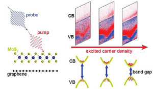 (Left) Schematic of pump-probe experiment: The pump pulse excites a heterostructure consisting of a single-layer of MoS2 on graphene. The excited state is probed via photoemission by an ultraviolet probe pulse. (Right) The upper panels present the excited signal measured in the MoS2 valence band (VB) and conduction band (CB). Red indicates excited electrons in the CB and a shift in the VB towards the CB. The lower panel presents a schematic of the observation: the bandgap in MoS2 renormalizes depending on the number of excited carriers generated with the pump pulse. (Credit: Soren Ulstrup)
In a recent experiment performed at the Artemis facility, a team of researchers used the time- and angle-resolved photoemission spectroscopy (TR-ARPES) technique to record ultrafast snapshots of how such a 2D MoS2-graphene heterostructure responds to an optical excitation by a tunable laser pump pulse.
Surprisingly, the band structure of the MoS2 layer changes dramatically once free carriers are excited in the valence and conduction bands of the material. The direct bandgap shrinks as the number of free carriers is increased due to the build-up of screening in the system. The number of free carriers and the following bandgap renormalization could be controlled by the power of the pump pulse in the experiment.
Since the size of the bandgap in a semiconductor determines its electronic and optical properties, the optical tunability discovered in the MoS2-graphene heterostructure in the experiment could open new avenues for the application of 2D optoelectronic devices, it is reckoned.
2D Metal dichalcogenide heterostructure Molybdenum disulfide
http://pubs.acs.org/doi/abs/10.1021/acsnano.6b02622
www.clf.stfc.ac.uk/CLF/Facilities/Artemis/12270.aspx


