


- News
15 July 2016
Flexible ultra-thin gallium arsenide photovoltaic devices
Researchers based in South Korea have developed a transfer-printing process to produce flexible gallium arsenide (GaAs) photovoltaic devices on metal without an interlayer adhesive [Juho Kim et al, Appl. Phys. Lett., vol108, p253101, 2016]. The researchers believe that such flexible devices could find application as wearable electric power sources deployed on the frames of a pair of glasses and/or fabric. Other possible uses include space applications and concentrator photovoltaics.
The team from Gwangju Institute of Science and Technology (GIST), Korea Photonics Technology Institute (KOPTI) and Yeungnam University claim the yields for the process are close to 100%.
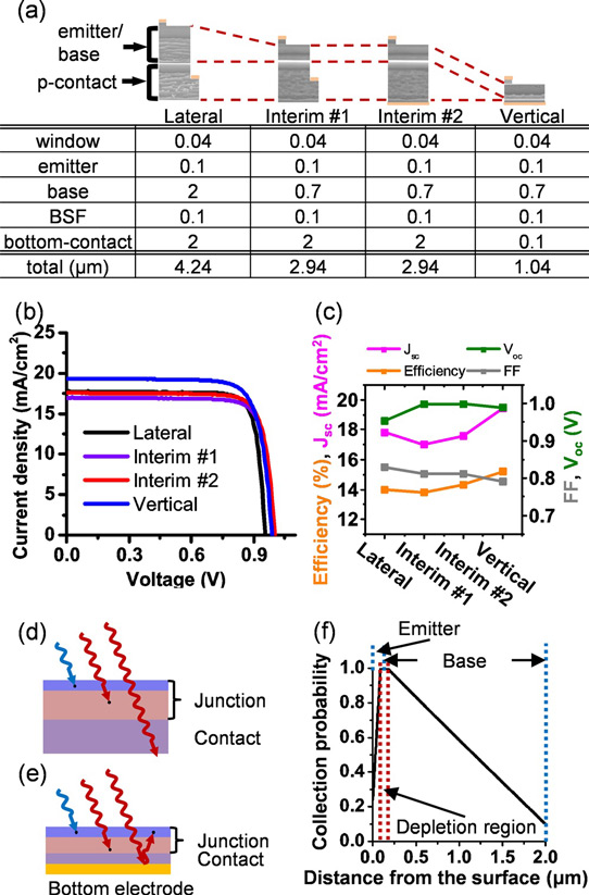
Figure 1: (a) Details of different solar microcell structures. (b) Measured current density (J)-voltage (V) curves under AM 1.5G illumination. (c) Measured short-circuit current density (Jsc), open-circuit voltage (Voc), fill factor (FF), and efficiency (η). (d) Schematic of photon dynamics in thick devices with most high-energy photons absorbed near surface, middle-energy photons absorbed at junction layer, and low-energy photons transmitted out of the microcell (a loss process). (e) Schematic of photon dynamics for ultra-thin device with bottom electrode reflecting non-absorbed photons. (f) Theoretical collection probability of GaAs solar cell.
The solar cell material was grown using low-pressure metal-organic chemical vapor deposition (LP-MOCVD) at 700°C. Various structures were grown, including an ultra-thin one with a thickness of a quarter that of thickest (Figure 1). "Thinner compound semiconductor devices, in addition, use less material and time and thus less cost when the epitaxial structures are grown," the team comments. The layers were GaAs, variously doped, except for a 0.1μm aluminium gallium arsenide (n-Al0.3Ga0.7As) back-surface field (BSF) layer.
Microcells were defined by photolithography and top electrodes of titanium/gold were deposited. Wet chemical mesa etching created 760μmx760μm active areas. A photoresist (PR) layer protected the devices during separation from the substrate by wet chemical etching of a sacrificial layer. Also, SU8 epoxy layers were used to reinforce the photoresist protection in some cases to avoid cracking where the microcells were ultra-thin.
The cells were transferred by film stamps constructed from polyimide (PI) and polydimethylsiloxane (PDMS). Before transfer, the bottom titanium/gold electrodes were deposited through a shadow mask that prevented metal being deposited on the sidewalls of the microcells, thus avoiding short circuiting between bottom and top contacts. The bottom electrode also constituted a light reflector in the ultra-thin cells, giving two passes for the photons to be absorbed.
The microcells were 'cold welded' onto metal electrodes on the receiver 12.5μm polyimide substrate by applying ~80kPa pressure at 170°C for 20 minutes (Figure 2). The photoresist protection helped avoid delamination when the film stamp was peeled away. The photoresist was removed with acetone.
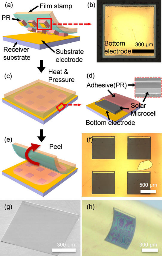
Figure 2: Fabrication of flexible vertical ultra-thin GaAs solar microcells with back reflector. (a) Film stamp with vertical GaAs microcells fabricated and isolated from epitaxially grown source wafers. (b) Bottom electrode, which also serves as back reflector, is deposited onto backside of ultra-thin vertical GaAs microcells. (c) After film stamp is brought into contact with receiver substrate. (d) Schematic and cross-sectional scanning electron microscope (SEM) image of microcell. (e) Peeling film stamp leaves vertical ultra-thin solar microcells on receiver substrate. (f) Optical microscope image of printed microcells after peeling film stamp. (g) SEM image of vertical solar microcell transfer-printed onto receiver substrate after PR removal. (h) Optical image of microcell wrapped on glass slide with a radius of 1mm.
The electrodes on the receiver substrate were 760μmx850μm rectangles. The microcells were encapsulated in 2μm SU8 epoxy and titanium/gold interconnects formed between the cells.
The ultra-thin sample had the highest Jsc of 19.4mA/cm2, while maintaining Voc near that of the thicker samples. The conversion efficiency of 15.2% for the ultra-thin device also exceeded that of the other structures.
The team attributes the improvements to the combined effects of the back reflector, and thinner base and bottom contact layers. The researchers add: "Most low-energy photons are absorbed at the junction (during the energy conversion process), but some of them are transmitted out of the junction (loss process). To reduce the loss, we can make the base thicker or re-route the photons to pass through the thinner junction using a back reflector."
The ultra-thin devices should also support more severe bending before breakage. The researchers found the ultra-thin arrays did not break after bending around 1mm-thick glass slides or the 1.4mm radius stem of a medical cleaning swab. Bending to 1.4mm radius and unbending up to a 1000 times gave no indication of degradation in the electrical performance, according to the team.
The researchers also interconnected seven cells in series with chromium/gold, giving a Voc of 6.8V, almost 7x that for a single cell (7x0.99V = 6.93V).
GaAs photovoltaic GaAs LP-MOCVD
http://dx.doi.org/10.1063/1.4954039
The author Mike Cooke is a freelance technology journalist who has worked in the semiconductor and advanced technology sectors since 1997.


