


- News
18 July 2016
Sodium flux route to free-standing gallium nitride substrates
Osaka University in Japan has developed a liquid phase epitaxy (LPE) process for the growth of gallium nitride (GaN) in a sodium (Na) flux with a small amount of carbon (C) that, with the addition of lithium (Li) and gallium, can also be used to dissolve sapphire (aluminium oxide, Al2O3), leaving free-standing GaN [Takumi Yamada et al, Appl. Phys. Express, vol9, p071002, 2016].
Without dissolving the sapphire substrate, the Ga-Na-C growth process results in cracks that the researchers attribute to stresses generated by cooling as a result of the mismatch in the thermal expansion coefficients of GaN and sapphire. By contrast, GaN with the sapphire substrate removed before cooling avoided cracking.
Free-standing GaN substrates are usually of higher quality than material left on the growth substrate due to the much lower dislocation densities of ~106/cm2, compared with ~108/cm2. Lower dislocation densities improve the performance of laser diodes, light-emitting diodes, and high-power, high-frequency electronic devices that harness the higher critical electric field, higher electron mobility and higher thermal conductivity of GaN.
The liquid phase epitaxy was performed on a 5μm GaN 'seed' on c-plane sapphire templates produced by hydride vapor phase epitaxy (HVPE) – see Figure 1. The liquid-source 20% Ga was combined with 80% Na and 0.05% graphite. Growth was carried out for between 72 and 200 hours at 870°C with nitrogen gas introduced at 4.0MPa. Before the sapphire dissolution, the temperature was raised to 900°C for 24 hours. Then Li and more Ga were added to the crucible. The extra Ga was designed to suppress Li evaporation. The amount of Li and Ga was 4-5 mol%. The substrate was removed after 24 hours dissolution. The dissolution process was optimized to avoid the formation of GaN polycrystals that can deposit on the grown GaN, reducing its crystallinity.
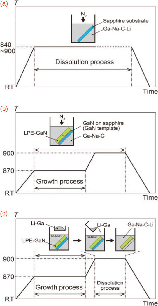
Figure 1: Diagrams of growth temperature and schematics of processes: (a) investigating sapphire solubility, (b) typical LPE, and (c) dissolving sapphire substrate after LPE.
X-ray analysis of the residues left in the crucible after the dissolution of the sapphire indicated that the Al2O3 reacted with Li to form Al, Li2O, LiAlO2, Li5AlO4 and Li9Al4, as reported by others.
The sample (1) with sapphire substrate had a GaN layer that was 1.9mm thick. For sample (2), where the sapphire substrate was removed by the Ga-Na-C-Li solution, the thickness was 1.0mm. The dislocation densities of both samples was around 106/cm2. X-ray analysis showed a reduced full-width at half-maximum (FWHM) of the 002 rocking curve for sample 2: 50arcsec compared with 100 arcsec for sample 1. The reduced crystal quality of sample 1 was possibly due to slight misorientation arising from cracks.
The researchers also believe that the sapphire dissolution technique would be useful for avoiding cracks in Na-flux growth on multipoint-seed GaN substrates. With such epitaxy, cracks form where there is a large contact interface between coalesced GaN and the sapphire substrate.
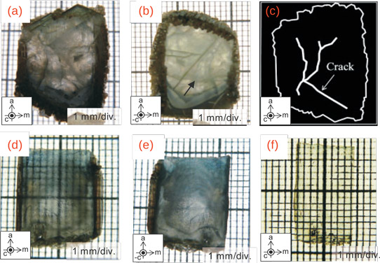
Figure 2: Transmission optical images of as-grown (a) c-face and (b) back-side surfaces of GaN crystal grown on c-GaN template without sapphire dissolution (sample 1). Black arrow indicates sapphire substrate. (c) Schematic of as-grown c-face surface. Transmission optical images of as-grown (d) c-face and (e) back-side surfaces of GaN crystal grown on c-GaN template, followed by sapphire dissolution (sample 2). (f) Optical image of sample 2 finished with chemical mechanical polishing.
The researchers write that "in the future, we will fabricate an extremely low-dislocation-density, low-curvature, and large-diameter GaN substrate with high yield by combining the Na-flux coalescence growth and sapphire dissolution techniques."
Sodium flux Free-standing GaN substrates GaN HVPE
http://doi.org/10.7567/APEX.9.071002
The author Mike Cooke is a freelance technology journalist who has worked in the semiconductor and advanced technology sectors since 1997.


