


- News
26 July 2016
Wafer bonding to integrate silicon, gallium arsenide, and gallium nitride
Researchers based in Singapore and the USA have been developing a process for bonding wafers that allows them to integrate gallium arsenide (GaAs), gallium nitride (GaN) and silicon (Si) CMOS layers [Kwang Hong Lee et al, Appl. Phys. Express vol9, p086501, 2016].
The researchers at the Singapore–MIT Alliance for Research and Technology (SMART) and Nanyang Technological University in Singapore and at Massachusetts Institute of Technology in the USA see the method as providing a route to further shrinking and scaling of CMOS and of functional diversification (Figure 1). III-V materials offer efficient light emission, high electron mobility, high critical fields, and so on.
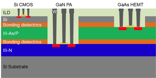
Figure 1: Schematic of hybrid integration with Si-CMOS (on SOI), high-frequency devices (e.g. HEMTs on III–As/P layer such as GaAs) and high-power devices (e.g. power amplifier on III–N layer such as GaN).
The team comments: "By this method, the functionalities of the materials used can be realized on a single Si platform (e.g. GaAs is more suitable for high-frequency high-electron-mobility transistor (HEMT) devices, GaN is more suitable on high-power devices, and inexpensive Si is more suitable for digital control circuitry)."
Ideally, III-V materials would be directly grown on silicon, but the high temperatures needed of up to 1350°C would likely destroy any silicon electronics that had previously been processed.
The procedure (Figure 2) began with a silicon-on-insulator (SOI) donor wafer on which a 500nm layer of silicon dioxide (SiO2) was applied using plasma-enhanced chemical vapor deposition (PECVD). The SOI structure consisted of 0.4μm of buried oxide (BOX) and 1.3μm of silicon. The BOX was created by thermal oxidation of the silicon substrate. The PECVD SiO2 was densified at 600°C in nitrogen to remove gas molecules and other byproducts incorporated by the deposition. The donor wafer was then planarized by chemical mechanical polishing (CMP).
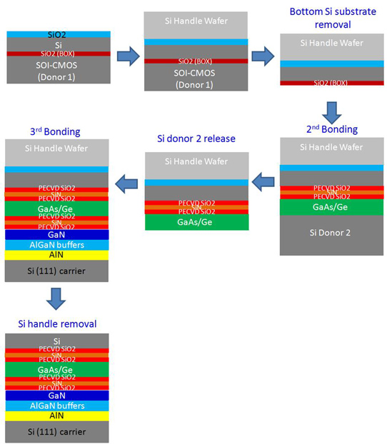
Figure 2: Process-flow scheme for triple-bond layer transfer.
The silicon carrier wafer was prepared by exposing the bond surfaces to oxygen plasma, rinsing in deionized water, and spin drying. The water rinse populates the surfaces with OH hydroxyl groups that initiate the bonding. The wafers were then brought together and annealed at 300°C in nitrogen for three hours to increase the bond strength. The silicon substrate of the SOI wafer was removed by mechanical grinding and wet etch. The BOX layer acted as an etch stop. The silicon handle wafer was protected from the etch by protective film.
The BOX layer was removed and replaced by PECVD SiO2 and silicon nitride (Si3N4). Both layers were densified and the SiO2 was subjected to CMP. The same PECVD layers were also applied to the second donor wafer that carried the germanium and GaAs layers. The bonding and donor silicon removal processes were similar to that of the SOI wafer. The germanium and GaAs layers were grown by metal-organic chemical vapor deposition (MOCVD) with the donor substrate offcut by 6° in the [110] direction.
The final carrier wafer consisted of GaN on (111) silicon to which the layers on the handle wafer were bonded with PECVD SiO2 and Si3N4 layers as before. The silicon handle was then removed using grinding and wet etch.
The bonding quality was inspected using infrared imaging since the component wafers are transparent to such wavelengths, making imperfections visible (Figure 3).
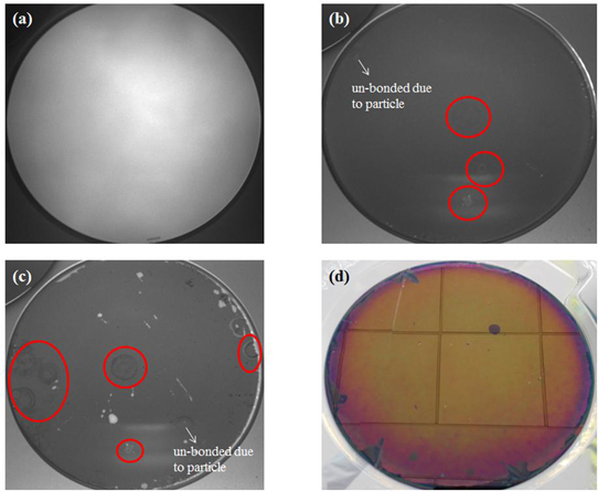
Figure 3: Infrared images of (a) first bonding of SOI and Si handle wafer, (b) second bonding to GaAs/Ge/Si substrate, and (c) third bonding to GaN/Si substrate. Red circles in (b) and (c) indicate defects from handle-wafer back side from wet etch. (d) Surface of SOI–GaAs/Ge/GaN/Si substrate after triple-bond layer transfer process.
The first bond was found to be "excellent" with no observable voids or particles. The second bond was less good, particularly near the edge. "The overall bonding quality is degraded by some trapped particles between the bonded pair and further improvement is required," the team reports.
Also, some defects were found on the handle-wafer back side due to incomplete protection by the film during wet etch of the donor silicon wafers. The third bond with the GaN/Si wafer suffered from the presence of particles and from problems originating from the unbonded areas of the second bond.
Transmission electron microscopy showed no microvoids in the bonds. "This indicates that a uniform and flawless bond is established successfully at the microscale level," the researchers write.
GaAs GaN Silicon CMOS Wafer bonding
http://doi.org/10.7567/APEX.9.086501
The author Mike Cooke is a freelance technology journalist who has worked in the semiconductor and advanced technology sectors since 1997.


