- News
6 July 2016
Correcting charge polarization calculations for III-nitrides
Researchers at University of California Santa Barbara (UCSB) and Rutgers University in the USA believe that charge polarization in III-nitride materials has not been adequately understood up to now [Cyrus E. Dreyer et al, Phys. Rev. X vol6, p021038, 2016]. Understanding charge polarization is vital for improving both light-emitting and electronic devices based on III-nitride (III-N) semiconductors, where the 'III' component consists of gallium (Ga), indium (In) and/or aluminum (Al).
For light-emitting devices, differences in charge polarization of the III-N chemical bond in the various epitaxial layers induce interface charges and electric fields that reduce the efficiency of electron-hole recombination into photons. This is commonly referred to as the quantum-confined Stark effect (QCSE).
By contrast, the effect of polarization is positive for electronics, where the charge polarization leads to the creation of a high-mobility confined 'two-dimensional' electron gases (2DEGs) near the interface between a GaN buffer and AlGaN or InAlN barrier layers. The 2DEG is used as a conduction channel controlled by a gate structure, giving a high-electron-mobility transistor (HEMT) operation with potential applications to power switching and high-frequency power amplification.
The III-nitrides used for light-emitting devices and for electronics have a wurtzite crystal structure and are typically grown along the c-axis by metal-organic chemical vapor deposition (MOCVD), molecular beam epitaxy (MBE), or hydride vapor phase epitaxy (HVPE) processes. The wutzite crystal structure is not inversion symmetric along the c-axis direction and this leads to the presence of polarization fields in heterostructures and quantum wells. The effect is worst when the growth is along the c-axis, as is almost always the case in commercial production.
One of the researchers, Chris van der Walle of UCSB, comments: "For the past two decades, analysis and modeling of these fields has been based on a set of calculated polarization constants for both spontaneous polarization (SP) and piezoelectric (PZ) polarization. While these published constants are not wrong 'per se', due to lack of clarity about how to implement them, they have been used incorrectly in all the work that has been done since then. The main paper containing these constants has been cited more than 1800 times, just to give an idea how widespread the use of these values is."
He adds: "We point out the error in the implementation, and we explain how to do the calculations correctly. We also explain why these errors have not been noticed to date: it is due to the fact that actually TWO errors have been made, which fortuitously approximately cancel. We show, however, that in some cases the correct implementation does lead to qualitatively different results. And of course, for such an important piece of physics, with such important applications, doing things correctly is important in its own right."
As van der Valle notes, charge polarization of wurtzite structures contains both spontaneous and strain-dependent (piezoelectric) components. Piezoelectricity has many sensor and transducer applications from the ability to create voltages from strain. In the reverse direction, mechanical effects can arise from applied voltages.
The first of the two problems concerns calculated coefficients for spontaneous polarization. These are defined with respect to a reference structure. The researchers claim that it is crucial to choose this structure such that it allows consistent comparisons between materials.
The other factor concerns the piezoelectric constants that need to take into account changes in interface area with strain. According to the team, the correct coefficients for this are the so-called 'improper' constants. 'Proper' constants arise from short-circuited conditions, while the 'improper' open-circuit condition includes strain modifications.
Traditionally, zincblende has been used as the reference structure for calculating spontaneous polarization. The UCSB/Rutgers researchers comment: "We show that, because the zincblende structure has a non-zero formal polarization, this method results in a spurious contribution to the spontaneous polarization differences between materials." The team believes that a better choice of reference is a layered hexagonal structure, for which no correction term is needed when calculating polarization discontinuities.
Separating spontaneous and piezoelectric contributions in experimental data is very difficult and theory is often used to give constants for use in simulations. The UCSB/Rutgers considerations are not restricted to III-nitrides, but the researchers chose to focus on them due to their technological importance.
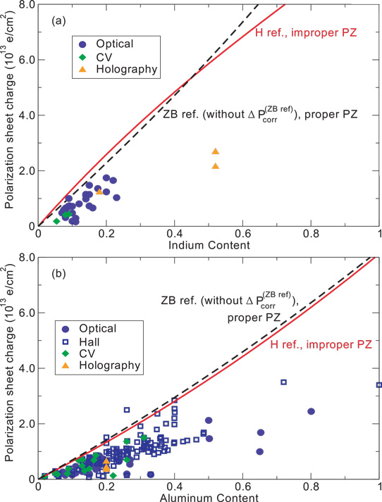
The researchers have compared their theory with experimental attempts to determine the sheet charge effects of polarization at InGaN/GaN and AlGaN/GaN interfaces (Figure 1). It is found that the conventional calculation gives very similar results to the new UCSB/Rutgers evaluation.

Figure 1: Absolute values for polarization sheet charges at (a) InGaN/GaN and (b) AlGaN/GaN interface as function of alloy content predicted from spontaneous polarization constants calculated using either zincblende (ZB) reference structure and proper piezoelectric constants (black dashed curve), or the hexagonal (H) reference structure and improper piezoelectric constants (red solid curve). Points are experimental values from literature.
With a few exceptions, both models give higher values than the widely scattered data. Experimental methods often make assumptions about sample structures – quantum well (QW) widths, compositions, profiles, etc – that deviate from reality.
The researchers comment on the InGaN/GaN data: "It has been shown recently that taking into account the deviations from ideal QW structures when interpreting experimental observations can account for the apparent discrepancy between the measurements and theoretical prediction of polarization fields. Such deviations are expected to be significant for InGaN/GaN because of the large lattice mismatch and the large difference in optimal growth temperatures for GaN and InGaN."
For AlGaN, "experimental uncertainties that can influence fields, such as incomplete strain relaxation in buffer layers, and differences in background doping" are cited as problems in matching data and models.
The researchers suggest that the small lattice mismatch between AlGaN and GaN also makes the difference less significant between the models. For InGaN/GaN, the difference becomes more significant at indium contents beyond 0.5 due to increasing lattice mismatch. Present growth technologies restrict high-quality InGaN to the indium-content range less than the order of 20%. "This will be important for the prediction of polarization fields in applications such as tunnel field-effect transistors based on thin, high-indium-content interlayers," the researchers suggest.

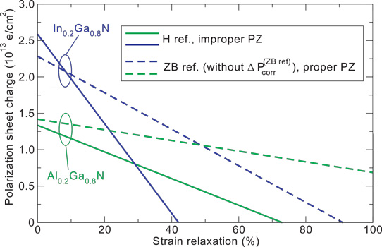
Figure 2: Absolute values for polarization sheet charges at In0.2Ga0.8N/GaN (blue) and Al0.2Ga0.8N/GaN (green) interface as a function of percentage strain relaxation: 0% relaxation corresponds to perfectly strained layers, 100% relaxation to an unstrained overlayer at its bulk lattice constant. Solid curves are proposed 'correct' implementation (H reference for SP and improper PZ constants); dashed curves are current practice (ZB reference for SP, without correction term, and proper PZ constants).
There are also larger expected effects where there is strain relaxation, according to the research (Figure 2), where there is a much faster fall-off in bound charge than the conventional approach would predict.
Polarization in III-nitride materials GaN HEMT MOCVD MBE HVPE
http://journals.aps.org/prx/abstract/10.1103/PhysRevX.6.021038
The author Mike Cooke is a freelance technology journalist who has worked in the semiconductor and advanced technology sectors since 1997.


