


- News
28 June 2016
Transfer printing of optically pumped III-V device on silicon-on-insulator
Ghent University/IMEC in Belgium and X-Celeprint in Ireland/USA claim "the first III-V optoelectronic components transfer printed on and coupled to a silicon photonic integrated circuit" [Andreas De Groote et al, Optics Express, vol24, p13754, 2016]. "This work forms a stepping stone towards the cost-effective integration of III-V optoelectronic components onto silicon photonic integrated circuits, including lasers, semiconductor optical amplifiers and electro-absorption modulators," the team adds.
The transfer method uses a polydimethylsiloxane (PDMS) elastomer stamp to pick up and place 'coupons' from a source to target in parallel. The coupons consist of thin-film materials or even completed devices. The adhesion of the materials to the stamp is determined by the speed of contact. A fast speed picks up the coupon and a slow speed releases it. By patterning the stamp, numbers of coupons can be picked up and placed in a magnified fashion on the target substrate (Figure 1). This allows efficient use and co-integration of different expensive III-V materials and device sources.
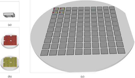
Figure 1: Area magnification in transfer printing III-V coupons from III-V source substrate to SOI target: (a) patterned stamp, (b) two source substrates with patterned coupons, and (c) SOI target substrate with four printed coupons of each source, top left.
The researchers comment: "While showing similarities with a pick-and-place technique, the main advantage of the transfer printing approach is that coupons can be transfer printed in a massively parallel way, by picking up and putting down large arrays of coupons at the same time. This allows for a high-throughput integration process."
The transferred coupons are ten to hundreds of microns in size, unlike in the usual wafer bonding methods where the dies are usually of the order of millimeters.
The coupons are transferred in a wafer-scale process, making alignment on SOI waveguide circuits non-critical, according to the researchers. Even so, with markers, a three-standard-deviation (3σ) alignment accuracy of ±1.5μm can be achieved.
The researchers transferred an indium gallium arsenide phosphide (InGaAsP) multi-quantum well (MQW) light-emitting device onto a silicon-on-insulator (SOI) chip with a processed waveguide circuit (Figure 2). The MQW was sandwiched between 60nm indium phosphide (InP) barriers. The total membrane thickness was 200nm.
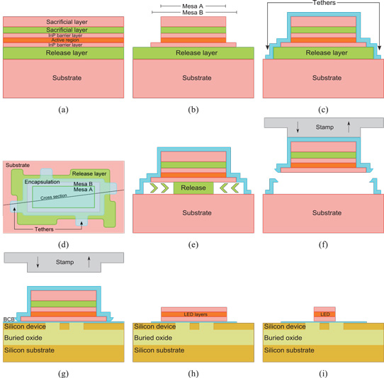
Figure 2: Process flow of transfer printed, optically pumped light-emitting device: (a) InP starting layer stack, (b) coupon patterning, (c) encapsulation and tether definition, (d) top view after encapsulation and tether definition. Further processing includes: (e) release etch, (f) pick-up of III-V coupon from source, (g) printing of coupon to SOI target, (h) removal of encapsulation and of sacrificial layers, (i) definition of light-emitting device.
The III-V material for the light-emitting device was grown on InP substrate. The sacrificial release layer was 1μm InGaAs. The top sacrificial layer was 100nm InGaAs, followed by 1μm InP. These top layers were designed to prevent buckling of the membrane when adhered to the transfer stamp.
The coupons were defined by a double mesa etch. A photoresist layer was used to protect the transfer layers while the release layer was under-etched. The coupons were transferred to the SOI wafer, which was coated with divinylsiloxane-bis-benzocyclobutene (DVS-BCB) polymer as an adhesive. The DVS-BCB was cured at 250°C for an hour. After the coupon was transferred and fixed, the photoresist was removed by oxygen plasma and the top sacrificial layers by a wet etch.
Different etch chemicals were tested for the release and finishing etch processes. The researchers comment: "The process should render a sufficiently strong bond to withstand strong acids and make sure that the III-V waveguide is close enough to the silicon waveguide in order to allow optical coupling through tapers."
The best release etch was found to be with cold iron chloride that delivered both full under-cutting of the layers and high selectivity against InP etch by a factor of more than 500. The wet etch took 2 hours to release the 40μm-wide coupons. The top sacrificial layers were removed with hydrochloric acid for InP and sulfuric acid mixed with hydrogen peroxide for the InGaAs.
The proof-of-principle setup consisted of a single-spatial-mode broadband light-emitting device integrated with SOI waveguides processed on 200mm wafers at IMEC's CMOS pilot line. In this case, the III-V device was pumped with optical power from a 1310nm laser directed through the SOI waveguide system (Figure 3).
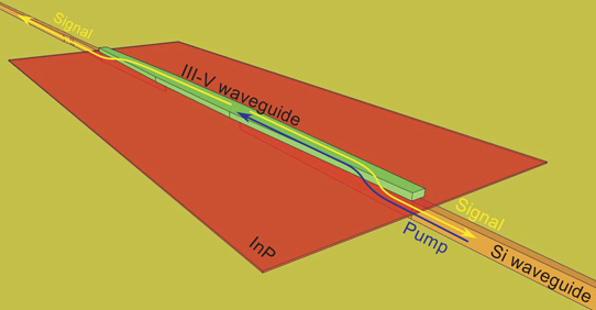
Figure 3: Optically pumped light-emitting device integration into SOI waveguide.
The pump light coupled up into the III-V membrane through an adiabatic taper structure developed at Ghent/IMEC [Sören Dhoore et al, Optics Express, vol24, p12976, 2016] designed to be highly tolerant in terms of alignment (Figure 4).
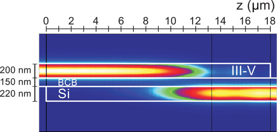
Figure 4: Side view of taper coupling structure intensity profile. 1550nm light is coupled adiabatically from III-V to silicon waveguide.
Measurements on the integrated III-V/SOI waveguide structure indicate a power efficiency of the emitted light at around 1550nm wavelength at the same order of magnitude as achieved with traditional III-V-on-silicon bonding. "The 3dB bandwidth of 130nm is large, and comparable as well to previously reported results," the team writes.
III-V optoelectronic components Transfer printing Silicon photonic integrated circuit InGaAsP SOI
http://dx.doi.org/10.1364/OE.24.013754
http://dx.doi.org/10.1364/OE.24.012976
The author Mike Cooke is a freelance technology journalist who has worked in the semiconductor and advanced technology sectors since 1997.


