


- News
22 June 2016
Probing potential to understand efficiency droop in InGaN LEDs
Korea University has sought to better understand the efficiency droop phenomenon that hits the performance of indium gallium nitride (InGaN) light-emitting diodes (LEDs) at higher currents by using a conducting diamond tip to probe the potential in the various layers of the device [Taewoong Kim et al, Appl. Phys. Lett., vol108, p231101, 2016].
The sample for the voltage probing consisted of 2.5μm of n-GaN, a 110nm superlattice (SL), an 80nm multiple quantum well (MQW), a 45nm electron-blocking layer (EBL), 60nm of p-GaN, and 60nm of indium tin oxide (ITO). These layers were grown on sapphire. The quantum wells consisted of In0.14Ga0.86N with an estimated 2.76eV bandgap.
The experimental setup consisted of the LED material mounted on its side and probed with a conductive diamond tip probe (Figure 1). A similar setup has been used by Korea University and LG Innotek to probe temperature variations in InGaN LEDs [E. Jung, et al, Appl. Phys. Lett. vol106, p041114, 2015]. Series resistance of the LED sample was estimated at 2.96Ω, based on current-voltage measurements. Maximum external quantum efficiency (EQE) was estimated to occur at 3.48A/cm2, according to Jung et al.
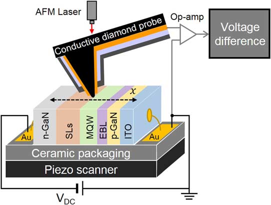
Figure 1: Schematic of experimental setup for measuring voltage profile on cross section of operating LED. Gold electrode of p-GaN side is grounded, measured voltage drops from 0V to negative value, approaching n-GaN.
The conductive diamond tip was designed for Seebeck microscopy. The conducting boron-doped diamond was grown by chemical vapor deposition (CVD). The tip radius was around 50nm. High contact pressure (~27GPa) was used to reduce the bandgap difference between the probe and sample, allowing electrical connection to be made. The contact diameter was around 25nm.
Measurements were carried out after about 10 minutes when the LED and probe had attained a thermal steady state. Potential profiles for four different current densities were averaged over 20 measurements to reduce noise effects (Figure 2).
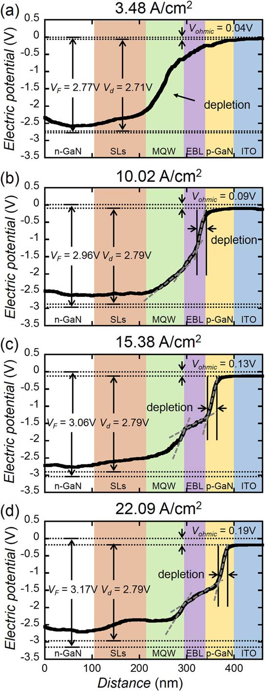
Figure 2: Averaged voltage profiles on cross section of operating LED obtained at (a) 3.48A/cm2, (b) 10.02A/cm2, (c) 15.38A/cm2, and (d) 22.09A/cm2.
The researchers interpret the kink in the profile as showing increased conductivity of electrons into the p-GaN region with increased current. These electrons then recombine non-radiatively in an electron 'depletion region'.
The researchers attribute the larger potential drop over the last part of the MQW region at higher currents (Figure 2d) as an indication that "more electrons and holes recombine in the last quantum well near the EBL as the current density increases."
Where efficiency droop begins to set in at lower current injection (Figure 2b), it is more difficult to see a kink and the researchers suggest that the electron depletion occurs then within the EBL.
At maximum EQE (Figure 2a), the researchers believe the electron depletion occurs in the MQW, as desired. "However, even the steepest voltage gradient in the profile shown in [Figure 2a] is relatively gentle compared with those shown in [Figures 2b-d]," the team writes. "This is because, at this lowest current density, the charge carriers deplete through a different mechanism (radiative recombination) to those occurring at other higher current densities (non-radiative recombination)."
The proportion of voltage drop across the MQW also varies with increasing current from ~50% of the total at 3.48A/cm2 to ~30% at 22A/cm2. "This directly shows that the proportion of the applied energy spent for radiative recombination decreases with increases in current density," the researchers comment.
The decrease in EQE in the same range is about 10%, compared with 40% ((50-30)/50) for the MQW potential drop fraction.
The researchers explain: "The actual electrochemical potential should be the average of the electrochemical potentials of electrons and holes weighted by carrier densities only. However, the measured voltage is the average of the electrochemical potentials weighted not only by the carrier densities but also by the carrier mobilities as well. As the mobility of electrons in GaN is much higher than that of holes, the measured voltage drop occurring in the EBL and p-GaN appears to be much greater than the actual potential energy drop."
The researchers give 50 as the approximate factor of electron/hole mobility in GaN.
LEDs InGaN InGaN LEDs Efficiency droop
http://dx.doi.org/10.1063/1.4953401
http://dx.doi.org/10.1063/1.4907177
The author Mike Cooke is a freelance technology journalist who has worked in the semiconductor and advanced technology sectors since 1997.


