


- News
15 June 2016
Thin-barrier quantum wells increase bandwidth of cyan light-emitting diode
Researchers based in Taiwan and USA have increased the modulation bandwidth of indium gallium nitride (InGaN) light-emitting diodes (LEDs) [Jin-Wei Shi, IEEE Electron Device Letters, published online 26 May 2016]. The enhanced bandwidth was achieved by reducing the barrier thickness in the multiple quantum well (MQW) active light-emitting region.
The team from National Central University (NCU) in Taiwan, University of California Santa Barbara (UCSB) in the USA, and National Cheng Kung University in Taiwan claims record 3dB electrical-to-optical (E-O) bandwidth values of nearly 1GHz, compared with other high-speed LEDs that only manage less than 0.5GHz.
One aim for the research was to boost data rates for visible-light communications and plastic optical fiber (POF) communications without significantly increasing light-source cost or energy consumption. Visible-light communication application could lead to ultra-broadband indoor wireless 'attocell' networks with large numbers of transmitter LEDs on the ceilings of rooms.
The researchers compared devices with standard 17nm and thin 5nm barriers (Figure 1). The LEDs were designed to be suitable for POF applications. The devices emitted around the cyan 480nm wavelength near the minimum loss window (less than 4dB/50m) of the poly(methyl methacrylate) (PMMA) thermoplastic that is commonly used for POF. The local minimum is actually around the 520nm green wavelength. A slightly deeper minimum is at 560nm (yellow). There is also a more lossy window around 650nm (red).
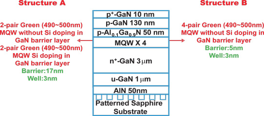
Figure 1: Conceptual cross-section of epitaxial layer standard (A) and thin-barrier (B) structures.
The researchers comment: "There are two major differences in the design of the active MQWs of these structures. One is the great reduction in thickness of the GaN barrier layer in the novel device structure from 17nm to 5nm. By thinning down the barrier layer, the total thickness of the active layer can also be reduced from 97nm to 37nm, which leads to an increase in the injected carrier density, radiative recombination rate, and modulation speed of the device. Furthermore, the thinness of the barrier layer should also improve the hole distribution among different wells and enhance the total output power."
With standard barriers, holes often find it difficult to distribute themselves effectively across MQW structures and tend to congregate in the well next to the p-type injection layers. Simulations suggested that the new thin barrier design could enhance hole transport across the MQW.
Another difference between the devices was that the standard LED had a partial n-type doping profile for the MQW in an effort to enhance modulation speeds and power output. Since the MQW region of the thin barrier device was much reduced, giving a greater applied electric field, the researchers believed that the new design did not need doping to achieve these effects.
The two device types were grown on patterned sapphire. Devices were fabricated on mesas etched down to the sapphire to avoid parasitic capacitance. The active area was around 50μm in diameter, while the device dimensions were 0.75mmx0.86mm (including contact pads on the sapphire substrate). By putting the metal pads on insulating sapphire, resistor-capacitor (RC) delays are minimized, enhancing bandwidth.
The performance of the two devices was similar, with the thin-barrier LED having a peak output power at room temperature of 1.7mW, compared with 1.5mW for the standard setup. The fall-off of peak power with raised temperature of 110°C was also similar: 20% for the standard LED and 19% with thin barriers. The researchers comment: "The comparable output power of these two structures under 110°C operation suggests that the thin barrier design does not significantly increase the probability of carriers escaping under high junction temperatures."
The 3dB E-O bandwidth for the new thin-barrier structure reached 0.96GHz at room temperature and 90mA bias (Figure 2). The standard device achieved 0.89GHz bandwidth. Both these values are claimed as being faster in terms of modulation compared with the best reported visible LEDs. Also, green InGaN laser diodes (LDs) have only achieved 0.4GHz bandwidth.
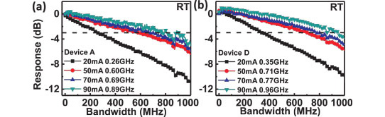
Figure 2: Bias-dependent E-O frequency responses for (a) standard device A and (b) thin-barrier device D at room temperatures.
The researchers comment: "The bandwidth performance of device D is over two times faster than that reported for the high-speed red [resonant-cavity] RCLEDs (0.35GHz) or GaN-based green (~500nm) LEDs and LDs (0.5GHz)."
While the LED performance is not as good as the recently reported 2.6GHz 3dB E-O bandwidth for a blue 450nm laser diode, the researchers point out that "the required driving current and fabrication cost of GaN laser diodes are both much higher than would be required for LED-based solutions." Also, PMMA POF becomes more lossy at 450nm.
At 110°C, the bandwidths at 60mA were 0.64GHz for the standard MQW LEDs and 0.71GHz for thin barriers. The relatively small degradations in power and bandwidth are seen as not serious.
The researchers write: "This is quite different from the behavior of the high-speed red RCLED, which shows bandwidth enhancement (110MHz to 130MHz) and serious degradation in the output power (~40%) when the temperature increases from 10°C to 70°C. The large bandgap offset in the active layer and the activation of the p-type dopant (Mg) in our III-nitride LED under high ambient temperatures act to suppress electron leakage and produce superior high-temperature performance over that of the GaAs-based high-speed red LED."
http://ieeexplore.ieee.org/xpl/articleDetails.jsp?arnumber=7479469
The author Mike Cooke is a freelance technology journalist who has worked in the semiconductor and advanced technology sectors since 1997.


