


- News
1 June 2016
Growing crystalline gallium nitride nanowires on flexible titanium foil
Paul-Drude-Institut für Festkörperelektronik in Germany has been studying self-assembled growth of gallium nitride (GaN) nanowires (NWs) on titanium (Ti) foil [Gabriele Calabrese et al, Appl. Phys. Lett., vol108, p202101, 2016].
Nanowire growth suffers from less problems due lattice mismatching, and the resulting material is generally more crystalline than for the usual epitaxial layers. Growth of GaN and related III-nitride materials on flexible substrates could open the way to low-cost roll-to-roll production methods for GaN optoelectronics. Metal foils also are attractive substrates in terms of enhanced thermal and electrical conductivity, along with optical reflectivity, compared with conventional substrates such as sapphire.
Ohio State University reported earlier this year on aluminium gallium nitride (AlGaN) ultraviolet light-emitting diodes on Ti and tantalum foils [reported at www.semiconductor-today.com/news_items/2016/apr/osu_290416.shtml].
The Paul-Drude-Institut GaN NWs were grown using solid source plasma-assisted molecular beam epitaxy (PA-MBE) on 25mmx25mm annealed polycrystalline Ti foil of 127μm thickness and ~50nm grain sizes. The foil was prepared by outgasing at 750°C and nitridation at 1000°C, giving a titanium nitride surface. The nitrogen source was plasma. The GaN NWs were grown at 730°C. The total growth took four hours.
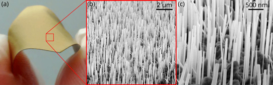
Figure 1: (a) Photograph of Ti foil after NW growth demonstrating high degree of flexibility. Also, bird's-eye view scanning electron micrographs of GaN NW ensemble grown on Ti foil with (b) low and (c) high magnification. Red square in (a) is not to scale.
The resulting NWs were vertically aligned (Figure 1). The regions between the wires were very rough: "The large surface roughness observed in between the NWs [see Fig. 1(c)] is tentatively attributed to interfacial reactions between Ga and Ti at non-nitridated regions of the substrate surface," the researchers write. The density of misoriented (i.e. non-vertical) wires was between one and two orders of magnitude lower than the vertically aligned ones.
Statistical analysis of electron micrographs suggested that the NW lengths and diameters were 1.14±0.37μm and 70±40nm, respectively. The NW density was 8.2x10⁷/cm2, about an order of magnitude lower than that for GaN NWs on (111) silicon. Due to the lower density, the NWs do not suffer from the coalescence problems seen in growth on silicon or aluminium nitride. The researchers comment: "Since the coalescence of GaN NWs is a source of inhomogeneous strain and results in the formation of non-radiative defects at the coalescence joints, the possibility to fabricate NW ensembles free of coalescence on Ti foils represents a decisive advantage over other substrates."
Out of 20 NWs studied closely, only one was found to have a basal stacking fault. Potassium hydroxide wet etching analysis showed the wires to be N-polar, as is usual for such structures grown by PA-MBE.
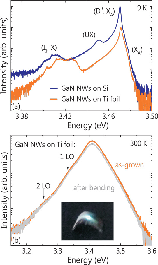
Figure 2: (a) Low-temperature (9K) PL spectrum of GaN NW ensemble grown on Ti foil. Corresponding spectrum of GaN NW ensemble on Si(111) is included for comparison. Spectra normalized and shifted vertically for clarity. (b) Room-temperature PL spectra of GaN NW ensemble grown on Ti foil for infinite and convex 4mm-radius curvature of substrate. Inset photograph of bent Ti foil taken during data acquisition.
The dominant peak for continuous-wave photoluminescence (PL) at 9K was at 3.471eV, corresponding to recombination of excitons bound to neutral oxygen donor atoms (D0 XA, Figure 2). This energy is the same as for bulk GaN, indicating the absence of homogeneous strain in the NWs. The full-width at half maximum (FWHM) value was 2.2meV. This is larger than the 1.5nm found for NWs grown on silicon. The researchers comment that FWHM values are determined by inhomogeneous strain and the energy distribution of donors as a result of varying distances from the NW sidewalls.
There was also a signal from the recombination of excitons bound to basal stacking faults between 3.40eV and 3.44eV. This was reduced by a factor of 50 compared with the 3.471eV peak. For NWs on silicon, the reduction factor is about 300, indicating a higher density of basal stacking faults in NWs on Ti foil. The researchers attribute the basal stacking faults to the significantly lower substrate temperature needed to promote NW nucleation on the titanium nitride surface.
A peak at 3.45eV is seen in the NWs on silicon, but is less pronounced on Ti foil. Such a peak has been associated with inversion domain boundaries (IDBs). "The absence of this transition suggests a reduced density of IDBs for growth on the Ti foil," the team writes.
The researchers also performed room-temperature photoluminescence measurements while bending the foil carrying the NWs. Little difference was seen in the spectrum before and after bending. The main peak at 3.41eV with 64meV FWHM was attributed to free A excitons. First- and second-order longitudinal optical (LO) phonon replicas were also seen. The researchers comment: "These observations demonstrate that the GaN NWs are well anchored to the substrate and do not detach upon bending."
GaN nanowires on titanium foil GaN PA-MBE
http://dx.doi.org/10.1063/1.4950707
The author Mike Cooke is a freelance technology journalist who has worked in the semiconductor and advanced technology sectors since 1997.


