


- News
29 June 2016
Bi-directional silicon carbide planar insulated-gate bipolar transistor
Rensselaer Polytechnic Institute and General Electric Global Research Center in the USA "experimentally demonstrate, for the first time, bi-directional 4H-silicon carbide planar gate, insulated-gate bipolar transistors (IGBTs) fabricated on 250μm-thick, lightly doped free-standing substrates" [Sauvik Chowdhury et al, IEEE Electron Device Letters, published online 15 June 2016].
The researchers see potential for their bi-directional (BD) IGBTs as switches that can control current in both directions with application in matrix or neutral point piloted multi-level converters. Compared with multi-component implementations, the BD-IGBT should offer reduced production costs and increased reliability.
The researchers used a wafer with lightly n-doped (N-) 250μm-thick epilayer grown on 4° off-axis N+ 4H SiC substrate. The growth wafer was removed to give a lightly doped free-standing substrate for the IGBT fabrication. Wafer-bonded silicon-based BD-IGBTs offer breakdown voltage ratings in the range 1.2-3.3kV. Unidirectional IGBTs produced using silicon carbide (SiC) technology have achieved breakdown voltage ratings up to 27kV.
The device was produced by lithographic patterning of planar gate metal-oxide-semiconductor (MOS) cells on both sides of the free-standing substrate (Figure 1). The gate insulator consisted of 75nm of low-pressure chemical vapor deposition (CVD) silicon dioxide dielectric. The oxide was annealed in nitric oxide (NO) gas at 1175°C for two hours. Junction termination extensions were achieved by aluminium implantation. Aluminium provides p-type doping in SiC. The individual IGBT devices were similar to unidirectional IGBTs reported earlier this year by Rensselaer [Sauvik Chowdhury et al, IEEE Electron Device Letters, vol37, p317, 2016]. The active area of the bi-directional IGBTs was 3.1x10⁻⁴cm2.
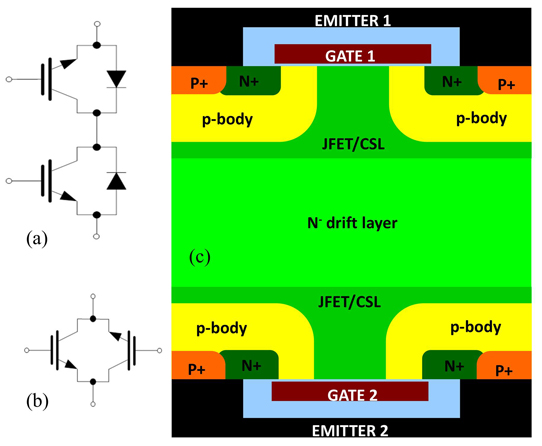
Figure 1: Bi-directional switches implemented using (a) conventional IGBTs and anti-parallel diodes (b) reverse blocking IGBTs and (c) schematic cross-section of monolithically integrated planar gate BD-IGBT.
With a collector current density of 50A/cm2, the Si-face forward voltage (VF) was 9.7V at room temperature and 11.5V at 150°C. The researchers claim the small positive temperature coefficient for VF is "attractive for stable current sharing among devices connected in parallel". The 11.5V VF compares with 27V for 15kV 4H-SiC power MOSFETs power switching devices reported by Cree/US Army Research Laboratory.
The differential specific on-resistance (ron,diff) of 140mΩ-cm2 was three times lower than the unmodulated drift layer. At higher temperatures, the decrease in mobility is compensated to some extent by an increase in carrier lifetimes and ionization of the aluminium acceptors. The ron,diff was only marginally higher: 160mΩ-cm2 at 150°C.
The voltage drops were higher in the reverse direction. Measured at a lower 10A/cm2 collector current density, VF was 9.5V at room temperature and 6.3V at 150°C. The ron,diff values were 600mΩ-cm2 and 400mΩ-cm2, respectively. The worse performance is attributed to a higher 13.7V threshold voltage for the C-face MOS gate, compared with 7.3V for the Si-face.
The researchers comment: "The threshold voltage on C-face also showed a faster rate of decrease with increasing temperature than Si-face. Higher VT, as well as the higher rate of decrease of VT with temperature, is indicative of a larger concentration of interface trapped charges (Qit) on C-face."
The team believes that through further optimization of the gate oxide process (reducing Qit on the C-face), a symmetric current-voltage performance could be achieved.
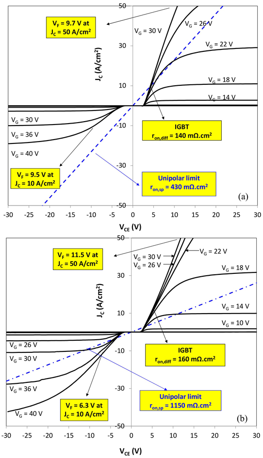
Figure 2: Typical experimental output current-voltage characteristics of fabricated 4HSiC BD-IGBT at (a) room temperature and (b) 150°C. Dashed line indicates calculated current-carrying capability of unmodulated drift layer. Cell pitch of measured device 17μm.
Breakdown measurements varied widely, with a maximum 7.2kV on the BD-IGBTs. Co-fabricated pin diodes had a higher 11kV breakdown. "This large variation in breakdown performance may be due to defects in the epilayer or surface passivation problems," the team writes. The expected breakdown characteristic of the drift layer was more than 17.5kV, giving a 15kV rating.
IGBTs 4H-silicon carbide planar gate InGaAsP
http://ieeexplore.ieee.org/xpl/articleDetails.jsp?arnumber=7492181
http://ieeexplore.ieee.org/xpl/articleDetails.jsp?arnumber=7390018
The author Mike Cooke is a freelance technology journalist who has worked in the semiconductor and advanced technology sectors since 1997.


