


- News
20 June 2016
Subwavelength micro-disk lasers on exact (001) silicon substrate
Researchers in Hong Kong and USA have been working on producing optically pumped micro-disk lasers on exact (001) silicon [Yating Wan et al, Appl. Phys. Lett., vol108, p221101, 2016]. The team from Hong Kong University of Science and Technology (HKUST) and University of California Santa Barbara (UCSB), Sandia National Laboratories and Harvard University in the USA writes: "We believe that the ultra-low threshold and small-footprint configurations provide significant insights and inspire future possibilities to incorporate efficient and compact laser sources on a CMOS-compatible platform."
The resulting devices had comparable performance to ones produced on gallium arsenide (GaAs) substrates. The use of on-axis substrates is more compatible with mainstream CMOS silicon electronics compared with wafer bonding or offcut substrates with germanium buffer or direct GaAs nucleation.
Lasing at around 1.3μm was achieved in 'subwavelength' 1μm-diameter devices. The researchers claim that subwavelength lasing had not been reported in devices produced on silicon before, although it had been on GaAs substrates.
A GaAs template layer was produced first, consisting of a 1μm layer of coalesced GaAs on V-grooved silicon (GoVS) grown by metal-organic chemical vapor deposition (MOCVD). The template layer did not contain antiphase layers and avoided the need for absorptive intermediate buffers.
Further layers (Figure 1) were grown by molecular beam epitaxy (MBE). The further layers included 1μm GaAs buffer and 600nm Al0.7Ga0.3As. The active region of the micro-disk laser consisted of five layers of InAs quantum dots (QDs) in InGaAs wells with GaAs barriers.
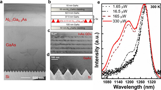
Figure 1: (a) Cross-sectional transmission electron micrograph (TEM) of micro-disk structure grown on GoVS substrate; (b) schematic epitaxial structure of material in disk region; (c) high-resolution TEM of five-stack InAs QDs; (d) cross-sectional TEM of V-grooved structure, showing defect trapping and localization; (e) room-temperature photoluminescence spectrum of as-grown structure at progressively higher excitations.
The researchers comment: "The good crystalline quality of the active device region is attributed to an effective defect trapping and reduction scheme through the V-grooved structure at the GaAs/Si hetero-interface."
In photoluminescence, the lowest-excited-state to ground-state emission was found to be in the 1.3μm optical telecom band. Higher excited states appeared in a high-energy/shorter-wavelength shoulder with increased pumping. "The wide inhomogeneous linewidth (about 20meV) allows for easy coupling into the resonant modes from small volume cavities with a large free spectral range (FSR)," the team adds.
The micro-disks were fabricated using lithography based on a colloidal suspension of 1μm-diameter silica beads, which were dispersed on the epitaxial material as a hard mask for inductively coupled plasma etch. The underlying Al0.7Ga0.3 was under-etched with hydrofluoric acid to create pedestals for the micro-disk structures.
Continuous-wave pumping with light from a 532nm diode laser at 10K showed evidence of lasing at a certain point in the form of narrowing of the linewidth. The estimated thresholds came in the range 35-67μW. The average was around 50μW, about 1.5x that for micro-disk layers on GaAs substrate (33μW). "The somewhat larger lasing thresholds on silicon are presumably related to crystalline defects (on the order of 1x10⁸/cm2 by plan-view transmission electron microscopy) leading to reduced QD modal gain," the researchers comment.
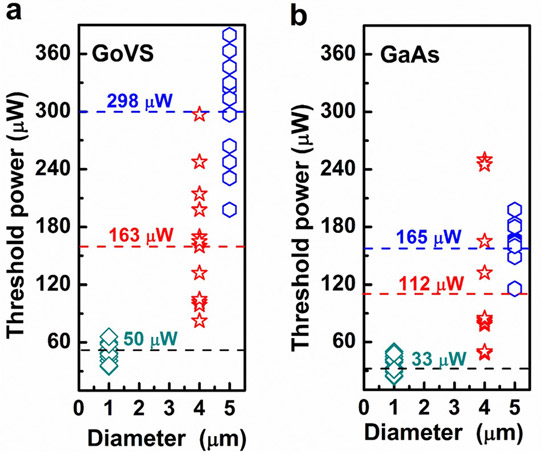
Figure 2: Threshold power as a function of disk diameter on GoVS template (a) and GaAs substrate (b). Dashed lines represent average threshold.
Larger disk diameters required a higher pump power (Figure 2). The researchers attribute this to the smaller mode separation and thus mode competition. "Due to the mode competition, micro-disk lasers with multi-mode lasing generally show larger thresholds. In addition, the larger disks have larger volumes of material to pump; in particular, the central region of the micro-disk absorbs pump power but has no spatial overlap with the [whispering gallery modes]," the team writes.
Subwavelength micro-disk lasers on silicon substrate Silicon substrate MOCVD MBE
http://dx.doi.org/10.1063/1.4952600
The author Mike Cooke is a freelance technology journalist who has worked in the semiconductor and advanced technology sectors since 1997.


